

Synthesis of Nanoscale Materials and Structures 269
photolithography
Photolithography, the process used to manufacture computer chips,
is able to produce features smaller than 100 nm (see Figure 8.25).
An oxidized silicon wafer is coated with a 1µm thick photoresist
layer, as in Figure 8.25a. A beam of UV light is incident on a mask,
allowing light to pass through the gaps. The light is then passed
through a set of lenses to reduce the pattern size, which is projected
onto the wafer, causing a photochemical reaction where it strikes
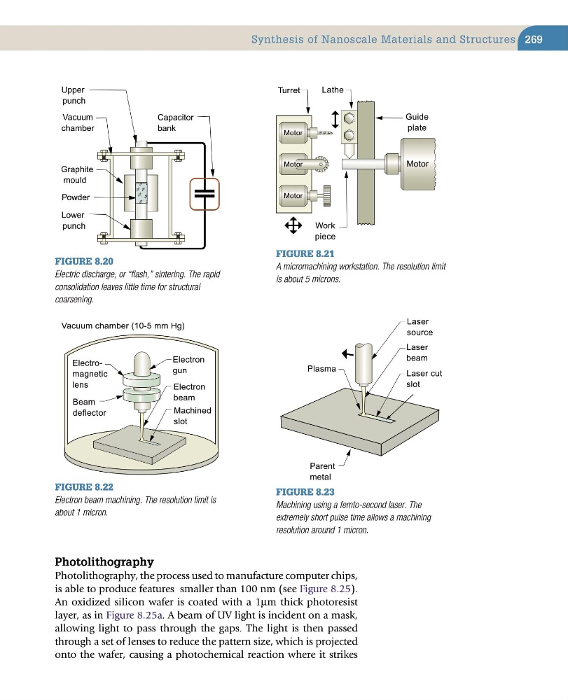
Figure 8.20
Electric discharge, or “flash,” sintering. The rapid
consolidation leaves little time for structural
coarsening.
Graphite
mould
Powder
Lower
punch
Upper
punch
Capacitor
bank
Vacuum
chamber
Figure 8.21
A micromachining workstation. The resolution limit
is about 5 microns.
Turret
Lathe
Work
piece
Guide
plate
Motor
Motor
Motor
Motor
Figure 8.22
Electron beam machining. The resolution limit is
about 1 micron.
Electron
gun
Machined
slot
Electron
beam
Electromagnetic
lens
Beam
deflector
Vacuum chamber (10-5 mm Hg)
Figure 8.23
Machining using a femto-second laser. The
extremely short pulse time allows a machining
resolution around 1 micron.
Parent
metal
Laser
source
Laser cut
slot
Laser
beam
Plasma
photolithography
Photolithography, the process used to manufacture computer chips,
is able to produce features smaller than 100 nm (see Figure 8.25).
An oxidized silicon wafer is coated with a 1µm thick photoresist
layer, as in Figure 8.25a. A beam of UV light is incident on a mask,
allowing light to pass through the gaps. The light is then passed
through a set of lenses to reduce the pattern size, which is projected
onto the wafer, causing a photochemical reaction where it strikes
Figure 8.20
Electric discharge, or “flash,” sintering. The rapid
consolidation leaves little time for structural
coarsening.
Graphite
mould
Powder
Lower
punch
Upper
punch
Capacitor
bank
Vacuum
chamber
Figure 8.21
A micromachining workstation. The resolution limit
is about 5 microns.
Turret
Lathe
Work
piece
Guide
plate
Motor
Motor
Motor
Motor
Figure 8.22
Electron beam machining. The resolution limit is
about 1 micron.
Electron
gun
Machined
slot
Electron
beam
Electromagnetic
lens
Beam
deflector
Vacuum chamber (10-5 mm Hg)
Figure 8.23
Machining using a femto-second laser. The
extremely short pulse time allows a machining
resolution around 1 micron.
Parent
metal
Laser
source
Laser cut
slot
Laser
beam
Plasma