

chapter 8 nanomaterials: Synthesis and characterization
262
electrodeposition
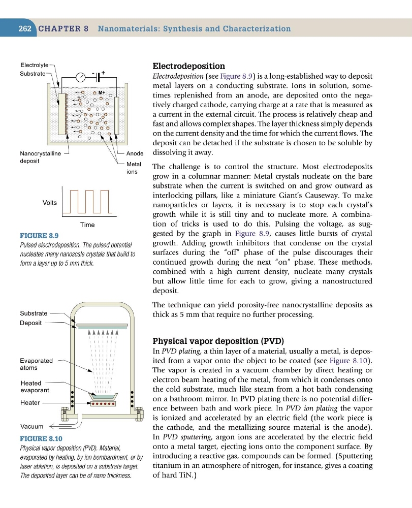
Electrodeposition (see Figure 8.9) is a long-established way to deposit
metal layers on a conducting substrate. Ions in solution, sometimes replenished from an anode, are deposited onto the negatively charged cathode, carrying charge at a rate that is measured as
a current in the external circuit. The process is relatively cheap and
fast and allows complex shapes. The layer thickness simply depends
on the current density and the time for which the current flows. The
deposit can be detached if the substrate is chosen to be soluble by
dissolving it away.
The challenge is to control the structure. Most electrodeposits
grow in a columnar manner: Metal crystals nucleate on the bare
substrate when the current is switched on and grow outward as
interlocking pillars, like a miniature Giant’s Causeway. To make
nanoparticles or layers, it is necessary is to stop each crystal’s
growth while it is still tiny and to nucleate more. A combination of tricks is used to do this. Pulsing the voltage, as suggested by the graph in Figure 8.9, causes little bursts of crystal
growth. Adding growth inhibitors that condense on the crystal
surfaces during the “off” phase of the pulse discourages their
continued growth during the next “on” phase. These methods,
combined with a high current density, nucleate many crystals
but allow little time for each to grow, giving a nanostructured
deposit.
The technique can yield porosity-free nanocrystalline deposits as
thick as 5 mm that require no further processing.
physical vapor deposition (pVd)
In PVD plating, a thin layer of a material, usually a metal, is deposited from a vapor onto the object to be coated (see Figure 8.10).
The vapor is created in a vacuum chamber by direct heating or
electron beam heating of the metal, from which it condenses onto
the cold substrate, much like steam from a hot bath condensing
on a bathroom mirror. In PVD plating there is no potential difference between bath and work piece. In PVD ion plating the vapor
is ionized and accelerated by an electric field (the work piece is
the cathode, and the metallizing source material is the anode).
In PVD sputtering, argon ions are accelerated by the electric field
onto a metal target, ejecting ions onto the component surface. By
introducing a reactive gas, compounds can be formed. (Sputtering
titanium in an atmosphere of nitrogen, for instance, gives a coating
of hard TiN.)
Figure 8.9
Pulsed electrodeposition. The pulsed potential
nucleates many nanoscale crystals that build to
form a layer up to 5 mm thick.
M+
+
-
Electrolyte
Substrate
Anode
Nanocrystalline
deposit
Volts
Time
Metal
ions
Figure 8.10
Physical vapor deposition (PVD). Material,
evaporated by heating, by ion bombardment, or by
laser ablation, is deposited on a substrate target.
The deposited layer can be of nano thickness.
Substrate
Vacuum
Deposit
Evaporated
atoms
Heater
Heated
evaporant
262
electrodeposition
Electrodeposition (see Figure 8.9) is a long-established way to deposit
metal layers on a conducting substrate. Ions in solution, sometimes replenished from an anode, are deposited onto the negatively charged cathode, carrying charge at a rate that is measured as
a current in the external circuit. The process is relatively cheap and
fast and allows complex shapes. The layer thickness simply depends
on the current density and the time for which the current flows. The
deposit can be detached if the substrate is chosen to be soluble by
dissolving it away.
The challenge is to control the structure. Most electrodeposits
grow in a columnar manner: Metal crystals nucleate on the bare
substrate when the current is switched on and grow outward as
interlocking pillars, like a miniature Giant’s Causeway. To make
nanoparticles or layers, it is necessary is to stop each crystal’s
growth while it is still tiny and to nucleate more. A combination of tricks is used to do this. Pulsing the voltage, as suggested by the graph in Figure 8.9, causes little bursts of crystal
growth. Adding growth inhibitors that condense on the crystal
surfaces during the “off” phase of the pulse discourages their
continued growth during the next “on” phase. These methods,
combined with a high current density, nucleate many crystals
but allow little time for each to grow, giving a nanostructured
deposit.
The technique can yield porosity-free nanocrystalline deposits as
thick as 5 mm that require no further processing.
physical vapor deposition (pVd)
In PVD plating, a thin layer of a material, usually a metal, is deposited from a vapor onto the object to be coated (see Figure 8.10).
The vapor is created in a vacuum chamber by direct heating or
electron beam heating of the metal, from which it condenses onto
the cold substrate, much like steam from a hot bath condensing
on a bathroom mirror. In PVD plating there is no potential difference between bath and work piece. In PVD ion plating the vapor
is ionized and accelerated by an electric field (the work piece is
the cathode, and the metallizing source material is the anode).
In PVD sputtering, argon ions are accelerated by the electric field
onto a metal target, ejecting ions onto the component surface. By
introducing a reactive gas, compounds can be formed. (Sputtering
titanium in an atmosphere of nitrogen, for instance, gives a coating
of hard TiN.)
Figure 8.9
Pulsed electrodeposition. The pulsed potential
nucleates many nanoscale crystals that build to
form a layer up to 5 mm thick.
M+
+
-
Electrolyte
Substrate
Anode
Nanocrystalline
deposit
Volts
Time
Metal
ions
Figure 8.10
Physical vapor deposition (PVD). Material,
evaporated by heating, by ion bombardment, or by
laser ablation, is deposited on a substrate target.
The deposited layer can be of nano thickness.
Substrate
Vacuum
Deposit
Evaporated
atoms
Heater
Heated
evaporant