

chaPter 7 nanomaterials: Properties
228
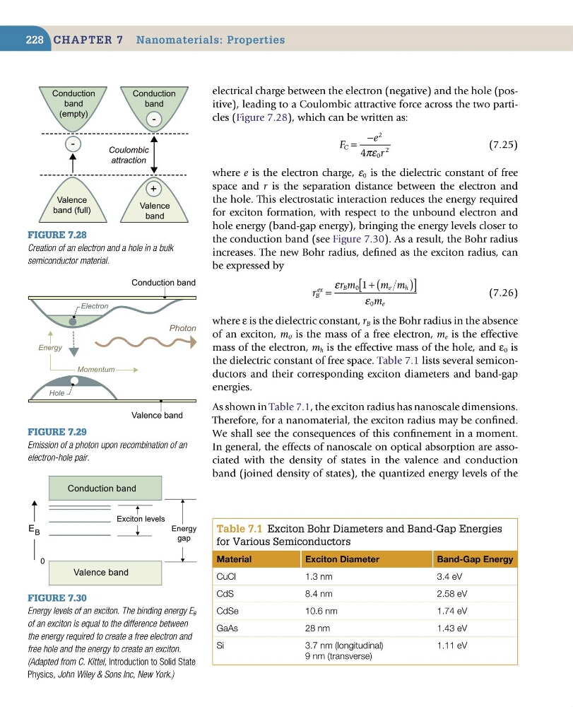
electrical charge between the electron (negative) and the hole (positive), leading to a Coulombic attractive force across the two particles (Figure 7.28), which can be written as:
F
e
r
C =
−
2
0
2
4πε
(7.25)
where e is the electron charge, ε 0 is the dielectric constant of free
space and r is the separation distance between the electron and
the hole. This electrostatic interaction reduces the energy required
for exciton formation, with respect to the unbound electron and
hole energy (band-gap energy), bringing the energy levels closer to
the conduction band (see Figure 7.30). As a result, the Bohr radius
increases. The new Bohr radius, defined as the exciton radius, can
be expressed by
r
r m
m m
m
B
ex
B
e
h
e
=
+ (
)
[
]
ε
ε
0
0
1
(7.26)
where ε is the dielectric constant, r B is the Bohr radius in the absence
of an exciton, m 0 is the mass of a free electron, m e is the effective
mass of the electron, m h is the effective mass of the hole, and ε 0 is
the dielectric constant of free space. Table 7.1 lists several semiconductors and their corresponding exciton diameters and band-gap
energies.
As shown in Table 7.1, the exciton radius has nanoscale dimensions.
Therefore, for a nanomaterial, the exciton radius may be confined.
We shall see the consequences of this confinement in a moment.
In general, the effects of nanoscale on optical absorption are associated with the density of states in the valence and conduction
band (joined density of states), the quantized energy levels of the
Figure 7.28
Creation of an electron and a hole in a bulk
semiconductor material.
Valence
band (full)
Valence
band
Conduction
band
Conduction
band
(empty)
Coulombic
attraction
+
-
-
Figure 7.29
Emission of a photon upon recombination of an
electron-hole pair.
Conduction band
Valence band
Photon
Electron
Hole
Energy
Momentum
Figure 7.30
Energy levels of an exciton. The binding energy E B
of an exciton is equal to the difference between
the energy required to create a free electron and
free hole and the energy to create an exciton.
(Adapted from C. Kittel, Introduction to Solid State
Physics, John Wiley & Sons Inc, New York.)
Exciton levels
Energy
gap
Conduction band
Valence band
E B
0
table 7.1 Exciton Bohr Diameters and Band-Gap Energies
for Various Semiconductors
Material
Exciton Diameter
Band-Gap Energy
CuCl
1.3 nm
3.4 eV
CdS
8.4 nm
2.58 eV
CdSe
10.6 nm
1.74 eV
GaAs
28 nm
1.43 eV
Si
3.7 nm (longitudinal)
9 nm (transverse)
1.11 eV
228
electrical charge between the electron (negative) and the hole (positive), leading to a Coulombic attractive force across the two particles (Figure 7.28), which can be written as:
F
e
r
C =
−
2
0
2
4πε
(7.25)
where e is the electron charge, ε 0 is the dielectric constant of free
space and r is the separation distance between the electron and
the hole. This electrostatic interaction reduces the energy required
for exciton formation, with respect to the unbound electron and
hole energy (band-gap energy), bringing the energy levels closer to
the conduction band (see Figure 7.30). As a result, the Bohr radius
increases. The new Bohr radius, defined as the exciton radius, can
be expressed by
r
r m
m m
m
B
ex
B
e
h
e
=
+ (
)
[
]
ε
ε
0
0
1
(7.26)
where ε is the dielectric constant, r B is the Bohr radius in the absence
of an exciton, m 0 is the mass of a free electron, m e is the effective
mass of the electron, m h is the effective mass of the hole, and ε 0 is
the dielectric constant of free space. Table 7.1 lists several semiconductors and their corresponding exciton diameters and band-gap
energies.
As shown in Table 7.1, the exciton radius has nanoscale dimensions.
Therefore, for a nanomaterial, the exciton radius may be confined.
We shall see the consequences of this confinement in a moment.
In general, the effects of nanoscale on optical absorption are associated with the density of states in the valence and conduction
band (joined density of states), the quantized energy levels of the
Figure 7.28
Creation of an electron and a hole in a bulk
semiconductor material.
Valence
band (full)
Valence
band
Conduction
band
Conduction
band
(empty)
Coulombic
attraction
+
-
-
Figure 7.29
Emission of a photon upon recombination of an
electron-hole pair.
Conduction band
Valence band
Photon
Electron
Hole
Energy
Momentum
Figure 7.30
Energy levels of an exciton. The binding energy E B
of an exciton is equal to the difference between
the energy required to create a free electron and
free hole and the energy to create an exciton.
(Adapted from C. Kittel, Introduction to Solid State
Physics, John Wiley & Sons Inc, New York.)
Exciton levels
Energy
gap
Conduction band
Valence band
E B
0
table 7.1 Exciton Bohr Diameters and Band-Gap Energies
for Various Semiconductors
Material
Exciton Diameter
Band-Gap Energy
CuCl
1.3 nm
3.4 eV
CdS
8.4 nm
2.58 eV
CdSe
10.6 nm
1.74 eV
GaAs
28 nm
1.43 eV
Si
3.7 nm (longitudinal)
9 nm (transverse)
1.11 eV