

227
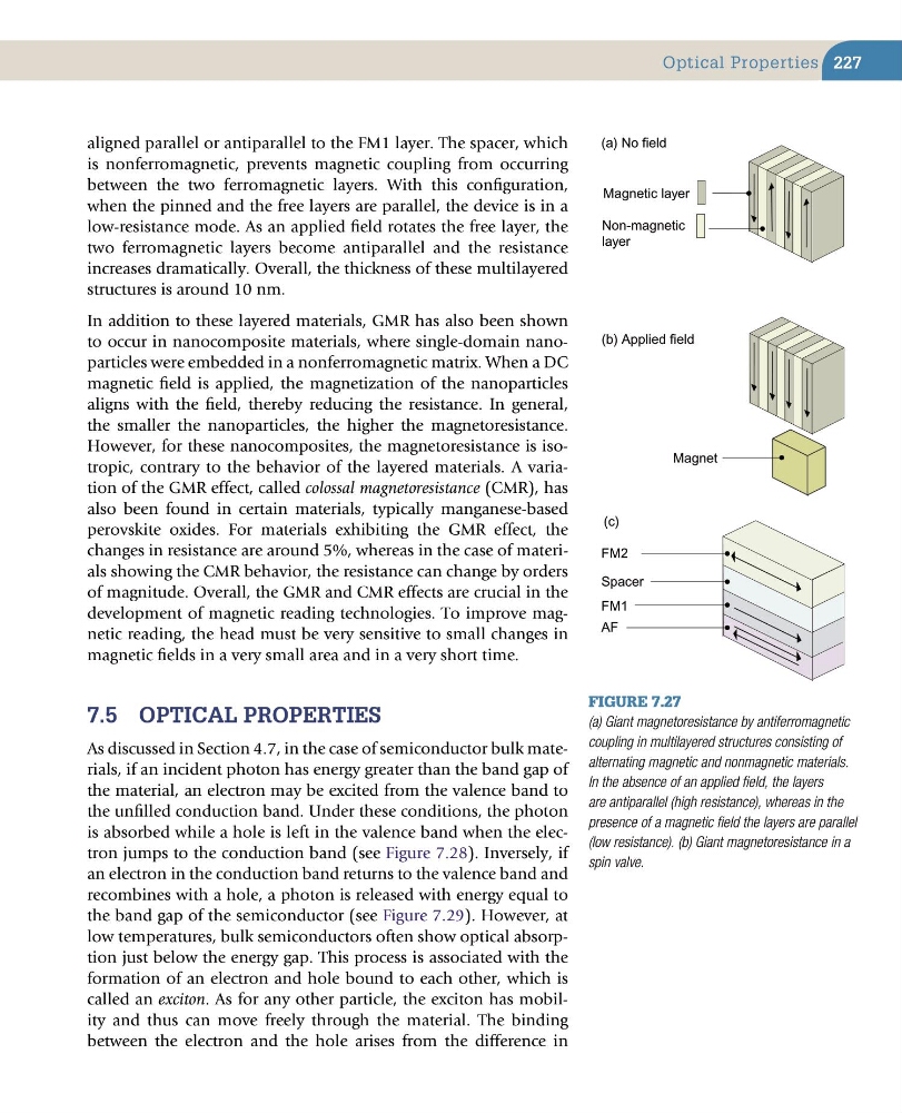
aligned parallel or antiparallel to the FM1 layer. The spacer, which
is nonferromagnetic, prevents magnetic coupling from occurring
between the two ferromagnetic layers. With this configuration,
when the pinned and the free layers are parallel, the device is in a
low-resistance mode. As an applied field rotates the free layer, the
two ferromagnetic layers become antiparallel and the resistance
increases dramatically. Overall, the thickness of these multilayered
structures is around 10 nm.
In addition to these layered materials, GMR has also been shown
to occur in nanocomposite materials, where single-domain nanoparticles were embedded in a nonferromagnetic matrix. When a DC
magnetic field is applied, the magnetization of the nanoparticles
aligns with the field, thereby reducing the resistance. In general,
the smaller the nanoparticles, the higher the magnetoresistance.
However, for these nanocomposites, the magnetoresistance is isotropic, contrary to the behavior of the layered materials. A variation of the GMR effect, called colossal magnetoresistance (CMR), has
also been found in certain materials, typically manganese-based
perovskite oxides. For materials exhibiting the GMR effect, the
changes in resistance are around 5%, whereas in the case of materials showing the CMR behavior, the resistance can change by orders
of magnitude. Overall, the GMR and CMR effects are crucial in the
development of magnetic reading technologies. To improve magnetic reading, the head must be very sensitive to small changes in
magnetic fields in a very small area and in a very short time.
7.5 oPtical ProPerties
As discussed in Section 4.7, in the case of semiconductor bulk materials, if an incident photon has energy greater than the band gap of
the material, an electron may be excited from the valence band to
the unfilled conduction band. Under these conditions, the photon
is absorbed while a hole is left in the valence band when the electron jumps to the conduction band (see Figure 7.28). Inversely, if
an electron in the conduction band returns to the valence band and
recombines with a hole, a photon is released with energy equal to
the band gap of the semiconductor (see Figure 7.29). However, at
low temperatures, bulk semiconductors often show optical absorption just below the energy gap. This process is associated with the
formation of an electron and hole bound to each other, which is
called an exciton. As for any other particle, the exciton has mobility and thus can move freely through the material. The binding
between the electron and the hole arises from the difference in
Figure 7.27
(a) Giant magnetoresistance by antiferromagnetic
coupling in multilayered structures consisting of
alternating magnetic and nonmagnetic materials.
In the absence of an applied field, the layers
are antiparallel (high resistance), whereas in the
presence of a magnetic field the layers are parallel
(low resistance). (b) Giant magnetoresistance in a
spin valve.
Non-magnetic
layer
Magnetic layer
Magnet
FM2
Spacer
FM1
AF
(a) No field
(b) Applied field
(c)
Optical Properties
aligned parallel or antiparallel to the FM1 layer. The spacer, which
is nonferromagnetic, prevents magnetic coupling from occurring
between the two ferromagnetic layers. With this configuration,
when the pinned and the free layers are parallel, the device is in a
low-resistance mode. As an applied field rotates the free layer, the
two ferromagnetic layers become antiparallel and the resistance
increases dramatically. Overall, the thickness of these multilayered
structures is around 10 nm.
In addition to these layered materials, GMR has also been shown
to occur in nanocomposite materials, where single-domain nanoparticles were embedded in a nonferromagnetic matrix. When a DC
magnetic field is applied, the magnetization of the nanoparticles
aligns with the field, thereby reducing the resistance. In general,
the smaller the nanoparticles, the higher the magnetoresistance.
However, for these nanocomposites, the magnetoresistance is isotropic, contrary to the behavior of the layered materials. A variation of the GMR effect, called colossal magnetoresistance (CMR), has
also been found in certain materials, typically manganese-based
perovskite oxides. For materials exhibiting the GMR effect, the
changes in resistance are around 5%, whereas in the case of materials showing the CMR behavior, the resistance can change by orders
of magnitude. Overall, the GMR and CMR effects are crucial in the
development of magnetic reading technologies. To improve magnetic reading, the head must be very sensitive to small changes in
magnetic fields in a very small area and in a very short time.
7.5 oPtical ProPerties
As discussed in Section 4.7, in the case of semiconductor bulk materials, if an incident photon has energy greater than the band gap of
the material, an electron may be excited from the valence band to
the unfilled conduction band. Under these conditions, the photon
is absorbed while a hole is left in the valence band when the electron jumps to the conduction band (see Figure 7.28). Inversely, if
an electron in the conduction band returns to the valence band and
recombines with a hole, a photon is released with energy equal to
the band gap of the semiconductor (see Figure 7.29). However, at
low temperatures, bulk semiconductors often show optical absorption just below the energy gap. This process is associated with the
formation of an electron and hole bound to each other, which is
called an exciton. As for any other particle, the exciton has mobility and thus can move freely through the material. The binding
between the electron and the hole arises from the difference in
Figure 7.27
(a) Giant magnetoresistance by antiferromagnetic
coupling in multilayered structures consisting of
alternating magnetic and nonmagnetic materials.
In the absence of an applied field, the layers
are antiparallel (high resistance), whereas in the
presence of a magnetic field the layers are parallel
(low resistance). (b) Giant magnetoresistance in a
spin valve.
Non-magnetic
layer
Magnetic layer
Magnet
FM2
Spacer
FM1
AF
(a) No field
(b) Applied field
(c)
Optical Properties