

chaPter 7 nanomaterials: Properties
226
electrons in a ferromagnet and the resistance provided by the presence of interfaces.
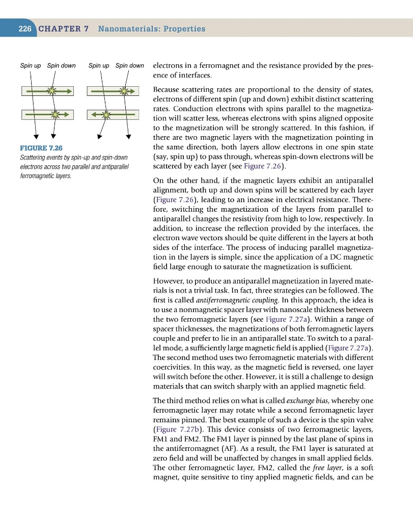
Because scattering rates are proportional to the density of states,
electrons of different spin (up and down) exhibit distinct scattering
rates. Conduction electrons with spins parallel to the magnetization will scatter less, whereas electrons with spins aligned opposite
to the magnetization will be strongly scattered. In this fashion, if
there are two magnetic layers with the magnetization pointing in
the same direction, both layers allow electrons in one spin state
(say, spin up) to pass through, whereas spin-down electrons will be
scattered by each layer (see Figure 7.26).
On the other hand, if the magnetic layers exhibit an antiparallel
alignment, both up and down spins will be scattered by each layer
(Figure 7.26), leading to an increase in electrical resistance. Therefore, switching the magnetization of the layers from parallel to
antiparallel changes the resistivity from high to low, respectively. In
addition, to increase the reflection provided by the interfaces, the
electron wave vectors should be quite different in the layers at both
sides of the interface. The process of inducing parallel magnetization in the layers is simple, since the application of a DC magnetic
field large enough to saturate the magnetization is sufficient.
However, to produce an antiparallel magnetization in layered materials is not a trivial task. In fact, three strategies can be followed. The
first is called antiferromagnetic coupling. In this approach, the idea is
to use a nonmagnetic spacer layer with nanoscale thickness between
the two ferromagnetic layers (see Figure 7.27a). Within a range of
spacer thicknesses, the magnetizations of both ferromagnetic layers
couple and prefer to lie in an antiparallel state. To switch to a parallel mode, a sufficiently large magnetic field is applied (Figure 7.27a).
The second method uses two ferromagnetic materials with different
coercivities. In this way, as the magnetic field is reversed, one layer
will switch before the other. However, it is still a challenge to design
materials that can switch sharply with an applied magnetic field.
The third method relies on what is called exchange bias, whereby one
ferromagnetic layer may rotate while a second ferromagnetic layer
remains pinned. The best example of such a device is the spin valve
(Figure 7.27b). This device consists of two ferromagnetic layers,
FM1 and FM2. The FM1 layer is pinned by the last plane of spins in
the antiferromagnet (AF). As a result, the FM1 layer is saturated at
zero field and will be unaffected by changes in small applied fields.
The other ferromagnetic layer, FM2, called the free layer, is a soft
magnet, quite sensitive to tiny applied magnetic fields, and can be
Figure 7.26
Scattering events by spin-up and spin-down
electrons across two parallel and antiparallel
ferromagnetic layers.
Spin up
Spin up
Spin down
Spin down
226
electrons in a ferromagnet and the resistance provided by the presence of interfaces.
Because scattering rates are proportional to the density of states,
electrons of different spin (up and down) exhibit distinct scattering
rates. Conduction electrons with spins parallel to the magnetization will scatter less, whereas electrons with spins aligned opposite
to the magnetization will be strongly scattered. In this fashion, if
there are two magnetic layers with the magnetization pointing in
the same direction, both layers allow electrons in one spin state
(say, spin up) to pass through, whereas spin-down electrons will be
scattered by each layer (see Figure 7.26).
On the other hand, if the magnetic layers exhibit an antiparallel
alignment, both up and down spins will be scattered by each layer
(Figure 7.26), leading to an increase in electrical resistance. Therefore, switching the magnetization of the layers from parallel to
antiparallel changes the resistivity from high to low, respectively. In
addition, to increase the reflection provided by the interfaces, the
electron wave vectors should be quite different in the layers at both
sides of the interface. The process of inducing parallel magnetization in the layers is simple, since the application of a DC magnetic
field large enough to saturate the magnetization is sufficient.
However, to produce an antiparallel magnetization in layered materials is not a trivial task. In fact, three strategies can be followed. The
first is called antiferromagnetic coupling. In this approach, the idea is
to use a nonmagnetic spacer layer with nanoscale thickness between
the two ferromagnetic layers (see Figure 7.27a). Within a range of
spacer thicknesses, the magnetizations of both ferromagnetic layers
couple and prefer to lie in an antiparallel state. To switch to a parallel mode, a sufficiently large magnetic field is applied (Figure 7.27a).
The second method uses two ferromagnetic materials with different
coercivities. In this way, as the magnetic field is reversed, one layer
will switch before the other. However, it is still a challenge to design
materials that can switch sharply with an applied magnetic field.
The third method relies on what is called exchange bias, whereby one
ferromagnetic layer may rotate while a second ferromagnetic layer
remains pinned. The best example of such a device is the spin valve
(Figure 7.27b). This device consists of two ferromagnetic layers,
FM1 and FM2. The FM1 layer is pinned by the last plane of spins in
the antiferromagnet (AF). As a result, the FM1 layer is saturated at
zero field and will be unaffected by changes in small applied fields.
The other ferromagnetic layer, FM2, called the free layer, is a soft
magnet, quite sensitive to tiny applied magnetic fields, and can be
Figure 7.26
Scattering events by spin-up and spin-down
electrons across two parallel and antiparallel
ferromagnetic layers.
Spin up
Spin up
Spin down
Spin down