

185
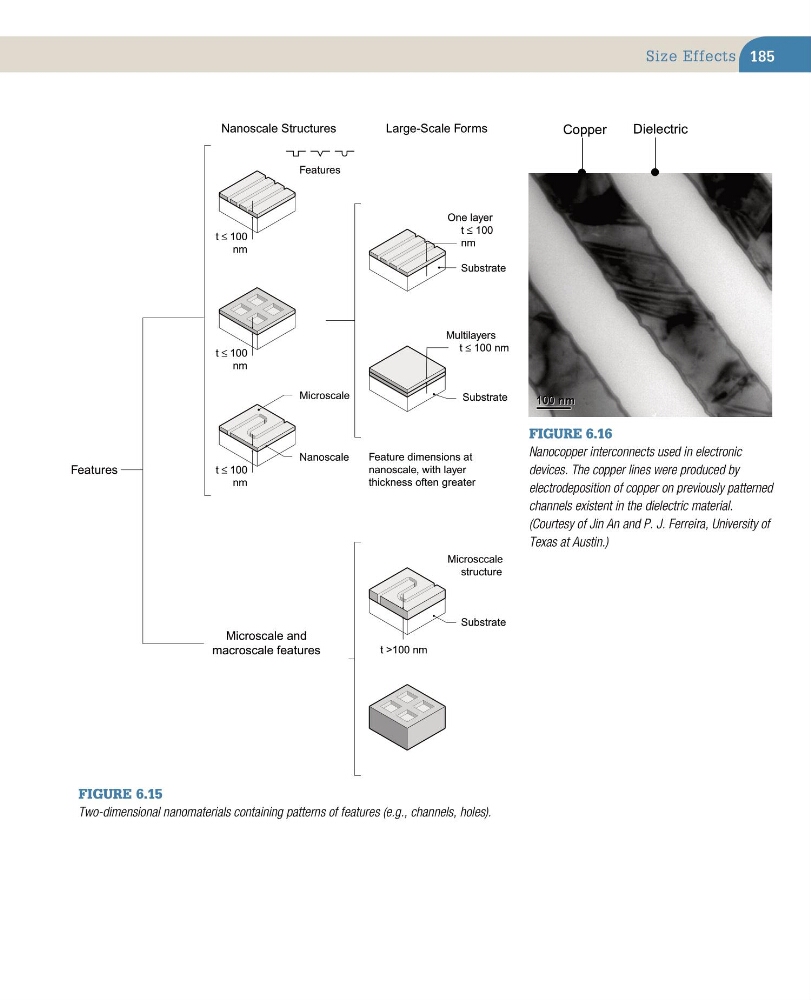
Figure 6.15
Two-dimensional nanomaterials containing patterns of features (e.g., channels, holes).
Figure 6.16
Nanocopper interconnects used in electronic
devices. The copper lines were produced by
electrodeposition of copper on previously patterned
channels existent in the dielectric material.
(Courtesy of Jin An and P. J. Ferreira, University of
Texas at Austin.)
t ≤ 100
nm
t ≤ 100
nm
t ≤ 100
nm
t >100 nm
One layer
t ≤ 100
nm
Substrate
Multilayers
t ≤ 100 nm
Microsccale
structure
Substrate
Feature dimensions at
nanoscale, with layer
thickness often greater
Microscale and
macroscale features
Nanoscale Structures
Large-Scale Forms
Microscale
Features
Nanoscale
Substrate
Features
Copper
Dielectric
Size Effects
Figure 6.15
Two-dimensional nanomaterials containing patterns of features (e.g., channels, holes).
Figure 6.16
Nanocopper interconnects used in electronic
devices. The copper lines were produced by
electrodeposition of copper on previously patterned
channels existent in the dielectric material.
(Courtesy of Jin An and P. J. Ferreira, University of
Texas at Austin.)
t ≤ 100
nm
t ≤ 100
nm
t ≤ 100
nm
t >100 nm
One layer
t ≤ 100
nm
Substrate
Multilayers
t ≤ 100 nm
Microsccale
structure
Substrate
Feature dimensions at
nanoscale, with layer
thickness often greater
Microscale and
macroscale features
Nanoscale Structures
Large-Scale Forms
Microscale
Features
Nanoscale
Substrate
Features
Copper
Dielectric
Size Effects