

The Internal Structure of Materials 101
and will be called interstitial atoms (different from self-interstitials).
Whether the impurities go to a substitutional or interstitial site
will depend on (1) atomic size, (2) crystal structure, (3) electronegativity, and (4) valence electrons. With respect to atomic size,
interstitial atoms are small compared with host atoms.
In covalent bonded materials, substitutional atoms can create
a unique imperfection in the electronic structure if the impurity
atom is from a group in the periodic table other than that of the
host atoms. An example is the addition of As or P (Group V) in
Si (Group IV; see Figure 4.25). Only four of five valence electrons
of these impurities can participate in the bonding, because there
are only four possible bonds with neighboring atoms. The extra
nonbonding electron is loosely bound to the region around the
impurity atom in a weak electrostatic interaction. Thus the binding
energy of this electron is relatively small, in which case it becomes
a free or conducting electron.
In polymers, the addition of impurities can also have significant
consequences. For example, natural rubber becomes cross-linked
when small amounts of sulfur (5%) are added. As a result, the
mechanical properties change dramatically. Natural rubber has a
tensile strength of 300 psi, whereas vulcanized rubber (sulfur addition) has a tensile strength of 3000 psi.
Now let’s discuss another class of defects called linear defects. These
defects, also called dislocations, are the main mechanism in operation when a material is deformed plastically. Currently, several
techniques are available for the direct observation of dislocations.
The transmission electron microscope (TEM) is probably the most
utilized in this respect.
Let’s look at the simplest case, the edge dislocation. Imagine the following sequence of events: (1) take a perfect crystal, (2) make a
cut in the crystal, (3) open the cut, and (4) insert an extra plane of
atoms (see Figure 4.26). The end result is an edge dislocation. These
dislocations are typically generated during processing or in service,
if subjected to enough stress. The presence and motion of dislocations dictate whether materials are ductile or brittle. Because metals
can easily generate and move dislocations, they are ductile. On the
other hand, ceramic materials have a high difficulty in nucleating
and moving dislocations due to the covalent/ionic character of the
bonds, and they are therefore brittle. One of the important parameters related to dislocations is the knowledge of the amount of
dislocation length per unit volume. This is called the dislocation
density and is given by
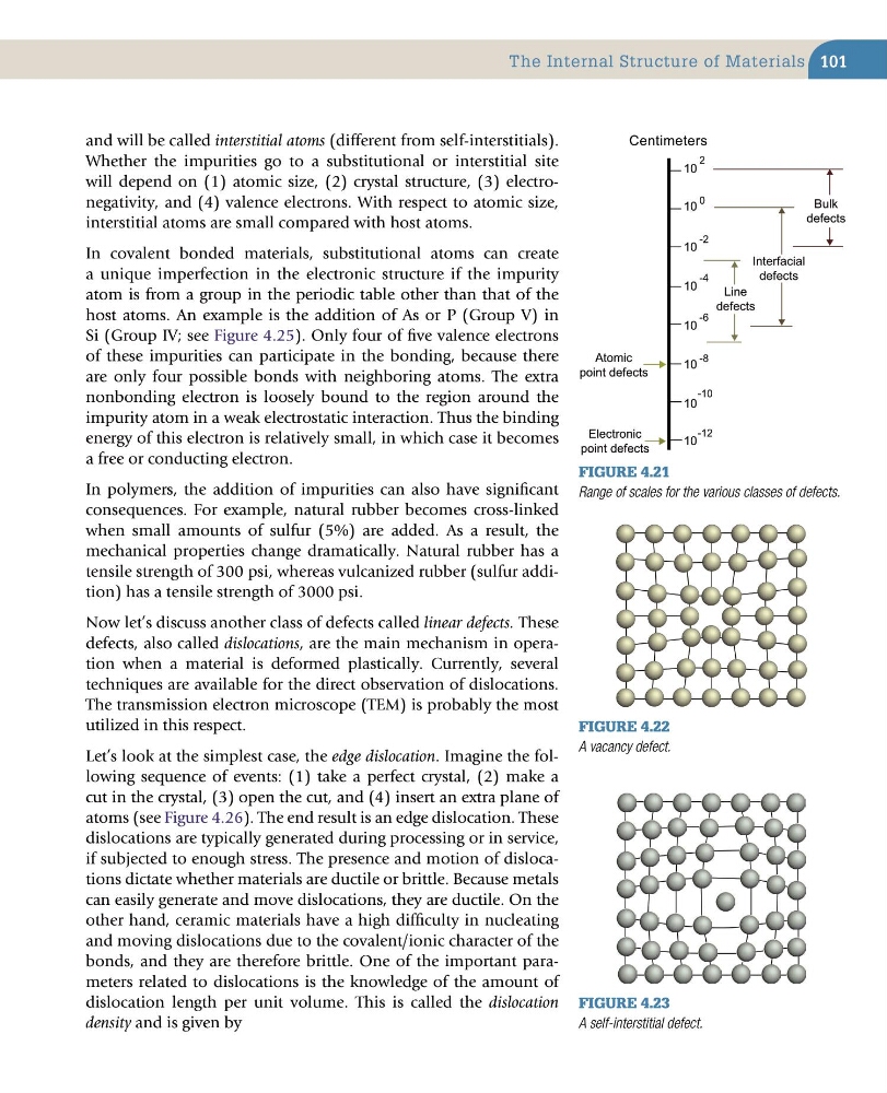
Figure 4.21
Range of scales for the various classes of defects.
Electronic
point defects
Atomic
point defects
Centimeters
Line
defects
Bulk
defects
Interfacial
defects
10
10
10
10
10
10
10
2
0
-2
-10
-8
-6
-4
10
-12
Figure 4.22
A vacancy defect.
Figure 4.23
A self-interstitial defect.
and will be called interstitial atoms (different from self-interstitials).
Whether the impurities go to a substitutional or interstitial site
will depend on (1) atomic size, (2) crystal structure, (3) electronegativity, and (4) valence electrons. With respect to atomic size,
interstitial atoms are small compared with host atoms.
In covalent bonded materials, substitutional atoms can create
a unique imperfection in the electronic structure if the impurity
atom is from a group in the periodic table other than that of the
host atoms. An example is the addition of As or P (Group V) in
Si (Group IV; see Figure 4.25). Only four of five valence electrons
of these impurities can participate in the bonding, because there
are only four possible bonds with neighboring atoms. The extra
nonbonding electron is loosely bound to the region around the
impurity atom in a weak electrostatic interaction. Thus the binding
energy of this electron is relatively small, in which case it becomes
a free or conducting electron.
In polymers, the addition of impurities can also have significant
consequences. For example, natural rubber becomes cross-linked
when small amounts of sulfur (5%) are added. As a result, the
mechanical properties change dramatically. Natural rubber has a
tensile strength of 300 psi, whereas vulcanized rubber (sulfur addition) has a tensile strength of 3000 psi.
Now let’s discuss another class of defects called linear defects. These
defects, also called dislocations, are the main mechanism in operation when a material is deformed plastically. Currently, several
techniques are available for the direct observation of dislocations.
The transmission electron microscope (TEM) is probably the most
utilized in this respect.
Let’s look at the simplest case, the edge dislocation. Imagine the following sequence of events: (1) take a perfect crystal, (2) make a
cut in the crystal, (3) open the cut, and (4) insert an extra plane of
atoms (see Figure 4.26). The end result is an edge dislocation. These
dislocations are typically generated during processing or in service,
if subjected to enough stress. The presence and motion of dislocations dictate whether materials are ductile or brittle. Because metals
can easily generate and move dislocations, they are ductile. On the
other hand, ceramic materials have a high difficulty in nucleating
and moving dislocations due to the covalent/ionic character of the
bonds, and they are therefore brittle. One of the important parameters related to dislocations is the knowledge of the amount of
dislocation length per unit volume. This is called the dislocation
density and is given by
Figure 4.21
Range of scales for the various classes of defects.
Electronic
point defects
Atomic
point defects
Centimeters
Line
defects
Bulk
defects
Interfacial
defects
10
10
10
10
10
10
10
2
0
-2
-10
-8
-6
-4
10
-12
Figure 4.22
A vacancy defect.
Figure 4.23
A self-interstitial defect.