

2.2. ENERGYBANDS
25
band at point Ts can become thermally excited to point r 6 in the conduction band
with no change in the wavevector k. The compounds GaAs, GaSb, InP, I d s , and
InSb and all the 11-VI compounds included in Table B.6 have direct gaps. In some
semiconductors such as Si and Ge the top of the valence band is at a position in the
Brillouin zone different from that for the bottom of the conduction band, and these
are called indirect-gap semiconductors.
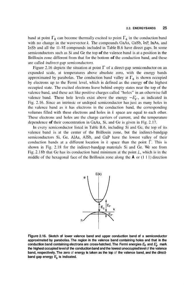
Figure 2.16 depicts the situation at point r of a direct-gap semiconductor on an
expanded scale, at temperatures above absolute zero, with the energy bands
approximated by parabolas. The conduction band valley at r 6 is shown occupied
by electrons up to the Fermi level, which is defined as the energy of the highest
occupied state. The excited electrons leave behind empty states near the top of the
valence band, and these act like positive charges called “holes” in an otherwise full
valence band. These hole levels exist above the energy -E;,, as indicated in
Fig. 2.16. Since an intrinsic or undoped semiconductor has just as many holes in
the valence band as it has electrons in the conduction band, the corresponding
volumes filled with these electrons and holes in k space are equal to each other.
These electrons and holes are the charge carriers of current, and the temperature
dependence of their concentration in GaAs, Si, and Ge is given in Fig. 2.17.
In every semiconductor listed in Table B.6, including Si and Ge, the top of its
valence band is at the center of the Brillouin zone, but the indirect-bandgap
semiconductors Si, Ge, AlAs, AlSb, and GaP have the lowest valley of their
conduction bands at a different location in k space than the point r. This is
shown in Fig. 2.18 for the indirect-bandgap materials Si and Ge. We see from
Fig. 2.18b that Ge has its conduction band minimum at the point L, which is in the
middle of the hexagonal face of the Brillouin zone along the A or (1 1 1) direction
Figure 2.16. Sketch of lower valence band and upper conduction band of a semiconductor
approximated by parabolas. The region in the valence band containing holes and that in the
conduction band containing electrons are cross-hatched. The Fermi energies EF and E;, mark
the highest occupied level of the conduction band and the lowest unoccupied level of the valence
band, respectively. The zero of energy is taken as the top of the valence band, and the directband gap energy Eg is indicated.
25
band at point Ts can become thermally excited to point r 6 in the conduction band
with no change in the wavevector k. The compounds GaAs, GaSb, InP, I d s , and
InSb and all the 11-VI compounds included in Table B.6 have direct gaps. In some
semiconductors such as Si and Ge the top of the valence band is at a position in the
Brillouin zone different from that for the bottom of the conduction band, and these
are called indirect-gap semiconductors.
Figure 2.16 depicts the situation at point r of a direct-gap semiconductor on an
expanded scale, at temperatures above absolute zero, with the energy bands
approximated by parabolas. The conduction band valley at r 6 is shown occupied
by electrons up to the Fermi level, which is defined as the energy of the highest
occupied state. The excited electrons leave behind empty states near the top of the
valence band, and these act like positive charges called “holes” in an otherwise full
valence band. These hole levels exist above the energy -E;,, as indicated in
Fig. 2.16. Since an intrinsic or undoped semiconductor has just as many holes in
the valence band as it has electrons in the conduction band, the corresponding
volumes filled with these electrons and holes in k space are equal to each other.
These electrons and holes are the charge carriers of current, and the temperature
dependence of their concentration in GaAs, Si, and Ge is given in Fig. 2.17.
In every semiconductor listed in Table B.6, including Si and Ge, the top of its
valence band is at the center of the Brillouin zone, but the indirect-bandgap
semiconductors Si, Ge, AlAs, AlSb, and GaP have the lowest valley of their
conduction bands at a different location in k space than the point r. This is
shown in Fig. 2.18 for the indirect-bandgap materials Si and Ge. We see from
Fig. 2.18b that Ge has its conduction band minimum at the point L, which is in the
middle of the hexagonal face of the Brillouin zone along the A or (1 1 1) direction
Figure 2.16. Sketch of lower valence band and upper conduction band of a semiconductor
approximated by parabolas. The region in the valence band containing holes and that in the
conduction band containing electrons are cross-hatched. The Fermi energies EF and E;, mark
the highest occupied level of the conduction band and the lowest unoccupied level of the valence
band, respectively. The zero of energy is taken as the top of the valence band, and the directband gap energy Eg is indicated.