

24
INTRODUCTION TO PHYSICS OF THE SOLID STATE
-8
26
x 7
-
-
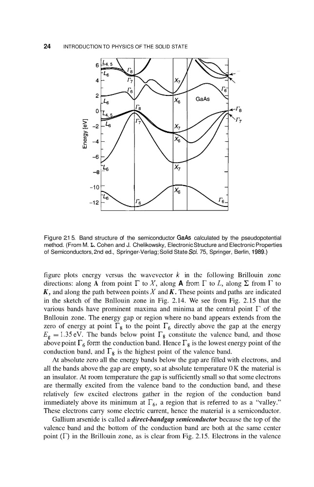
Figure 2.1 5. Band structure of the semiconductor GaAs calculated by the pseudopotential
method. (From M. L. Cohen and J. Chelikowsky, Electronic Structure and Electronic Properties
of Semiconductors, 2nd ed., Springer-Verlag; Solid State Sci. 75, Springer, Berlin, 1989.)
-
x6
-10 -
figure plots energy versus the wavevector k in the following Brillouin zone
directions: along A from point r to X , along A from to L, along C from r to
K , and along the path between points X and K . These points and paths are indicated
in the sketch of the Bnllouin zone in Fig. 2.14. We see from Fig. 2.15 that the
various bands have prominent maxima and minima at the central point r of the
Bnllouin zone. The energy gap or region where no band appears extends from the
zero of energy at point Ts to the point r 6 directly above the gap at the energy
Eg = 1.35eV. The bands below point Ts constitute the valence band, and those
above point r 6 form the conduction band. Hence Ts is the lowest energy point of the
conduction band, and Ts is the highest point of the valence band.
At absolute zero all the energy bands below the gap are filled with electrons, and
all the bands above the gap are empty, so at absolute temperature 0 K the material is
an insulator. At room temperature the gap is sufficiently small so that some electrons
are thermally excited from the valence band to the conduction band, and these
relatively few excited electrons gather in the region of the conduction band
immediately above its minimum at r6, a region that is referred to as a “valley.”
These electrons carry some electric current, hence the material is a semiconductor.
Gallium arsenide is called a direct-bandgap semiconductor because the top of the
valence band and the bottom of the conduction band are both at the same center
point (r) in the Brillouin zone, as is clear from Fig. 2.15. Electrons in the valence
INTRODUCTION TO PHYSICS OF THE SOLID STATE
-8
26
x 7
-
-
Figure 2.1 5. Band structure of the semiconductor GaAs calculated by the pseudopotential
method. (From M. L. Cohen and J. Chelikowsky, Electronic Structure and Electronic Properties
of Semiconductors, 2nd ed., Springer-Verlag; Solid State Sci. 75, Springer, Berlin, 1989.)
-
x6
-10 -
figure plots energy versus the wavevector k in the following Brillouin zone
directions: along A from point r to X , along A from to L, along C from r to
K , and along the path between points X and K . These points and paths are indicated
in the sketch of the Bnllouin zone in Fig. 2.14. We see from Fig. 2.15 that the
various bands have prominent maxima and minima at the central point r of the
Bnllouin zone. The energy gap or region where no band appears extends from the
zero of energy at point Ts to the point r 6 directly above the gap at the energy
Eg = 1.35eV. The bands below point Ts constitute the valence band, and those
above point r 6 form the conduction band. Hence Ts is the lowest energy point of the
conduction band, and Ts is the highest point of the valence band.
At absolute zero all the energy bands below the gap are filled with electrons, and
all the bands above the gap are empty, so at absolute temperature 0 K the material is
an insulator. At room temperature the gap is sufficiently small so that some electrons
are thermally excited from the valence band to the conduction band, and these
relatively few excited electrons gather in the region of the conduction band
immediately above its minimum at r6, a region that is referred to as a “valley.”
These electrons carry some electric current, hence the material is a semiconductor.
Gallium arsenide is called a direct-bandgap semiconductor because the top of the
valence band and the bottom of the conduction band are both at the same center
point (r) in the Brillouin zone, as is clear from Fig. 2.15. Electrons in the valence