

9.3. SIZE AND DIMENSIONALITY EFFECTS
233
between grains, and a stacking fault arising from a sudden change in the stacking
arrangement of close-packed planes. A vacant space called a pore, a cluster of
vacancies, and a precipitate of a second phase are three-dimensional defects. All of
these can bring about the scattering of electrons, and thereby limit the electrical
conductivity. Some nanostructures are too small to have internal defects.
Another size effect arises from the level of doping of a semiconductor. For typical
doping levels of lOI4 to 10" donors/cm3 a quantum-dot cube lOOnm on a side
would have, on the average, from lo-' to lo3 conduction electrons. The former
figure of lo-' electrons per cubic centimeter means that on the average only 1
quantum dot in 10 will have one of these electrons. A smaller quantum-dot cube
only 10 nm on a side would have, on the average 1 electron for the 1OIs doping level,
and be very unlikely to have any conduction electrons for the lOI4 doping level. A
similar analysis can be made for quantum wires and quantum wells, and the results
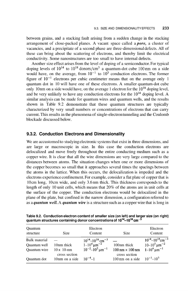
shown in Table 9.2 demonstrate that these quantum structures are typically
characterized by very small numbers or concentrations of electrons that can carry
current. This results in the phenomena of single-electron tunneling and the Coulomb
blockade discussed below.
9.3.2. Conduction Electrons and Dimensionality
We are accustomed to studying electronic systems that exist in three dimensions, and
are large or macroscopic in size. In this case the conduction electrons are
delocalized and move freely throughout the entire conducting medium such as a
copper wire. It is clear that all the wire dimensions are very large compared to the
distances between atoms. The situation changes when one or more dimensions of
the copper becomes so small that it approaches several times the spacings between
the atoms in the lattice. When this occurs, the delocalization is impeded and the
electrons experience confinement. For example, consider a flat plate of copper that is
10 cm long, 10 cm wide, and only 3.6 nm thick. This thickness corresponds to the
length of only 10 unit cells, which means that 20% of the atoms are in unit cells at
the surface of the copper. The conduction electrons would be delocalized in the
plane of the plate, but confined in the narrow dimension, a configuration referred to
as a quantum well. A quantum wire is a structure such as a copper wire that is long in
Table 9.2. Conduction electron content of smaller size (on left) and larger size (on right)
quantum structures containing donor concentrations of 10'4-10'8~m-3
Quantum
structure
Size
Bulk material
-
Quantum well
10 nm thick
Quantum wire 10 x 10-nm
Quantum dot
cross section
10 nm on a side
Electron
Electron
Content
Size
Content
1014-10'8cm-3
-
1014-1018Cm-3
1-io4 pm-2
100 nm thick
10-io5 pm-2
10-2-102pm-'
lOOnm x 1OOnm 1-104pm-'
10-~-1
lOOnm on a side 10-'-103
cross section
233
between grains, and a stacking fault arising from a sudden change in the stacking
arrangement of close-packed planes. A vacant space called a pore, a cluster of
vacancies, and a precipitate of a second phase are three-dimensional defects. All of
these can bring about the scattering of electrons, and thereby limit the electrical
conductivity. Some nanostructures are too small to have internal defects.
Another size effect arises from the level of doping of a semiconductor. For typical
doping levels of lOI4 to 10" donors/cm3 a quantum-dot cube lOOnm on a side
would have, on the average, from lo-' to lo3 conduction electrons. The former
figure of lo-' electrons per cubic centimeter means that on the average only 1
quantum dot in 10 will have one of these electrons. A smaller quantum-dot cube
only 10 nm on a side would have, on the average 1 electron for the 1OIs doping level,
and be very unlikely to have any conduction electrons for the lOI4 doping level. A
similar analysis can be made for quantum wires and quantum wells, and the results
shown in Table 9.2 demonstrate that these quantum structures are typically
characterized by very small numbers or concentrations of electrons that can carry
current. This results in the phenomena of single-electron tunneling and the Coulomb
blockade discussed below.
9.3.2. Conduction Electrons and Dimensionality
We are accustomed to studying electronic systems that exist in three dimensions, and
are large or macroscopic in size. In this case the conduction electrons are
delocalized and move freely throughout the entire conducting medium such as a
copper wire. It is clear that all the wire dimensions are very large compared to the
distances between atoms. The situation changes when one or more dimensions of
the copper becomes so small that it approaches several times the spacings between
the atoms in the lattice. When this occurs, the delocalization is impeded and the
electrons experience confinement. For example, consider a flat plate of copper that is
10 cm long, 10 cm wide, and only 3.6 nm thick. This thickness corresponds to the
length of only 10 unit cells, which means that 20% of the atoms are in unit cells at
the surface of the copper. The conduction electrons would be delocalized in the
plane of the plate, but confined in the narrow dimension, a configuration referred to
as a quantum well. A quantum wire is a structure such as a copper wire that is long in
Table 9.2. Conduction electron content of smaller size (on left) and larger size (on right)
quantum structures containing donor concentrations of 10'4-10'8~m-3
Quantum
structure
Size
Bulk material
-
Quantum well
10 nm thick
Quantum wire 10 x 10-nm
Quantum dot
cross section
10 nm on a side
Electron
Electron
Content
Size
Content
1014-10'8cm-3
-
1014-1018Cm-3
1-io4 pm-2
100 nm thick
10-io5 pm-2
10-2-102pm-'
lOOnm x 1OOnm 1-104pm-'
10-~-1
lOOnm on a side 10-'-103
cross section