

232
QUANTUM WELLS, WIRES, AND DOTS
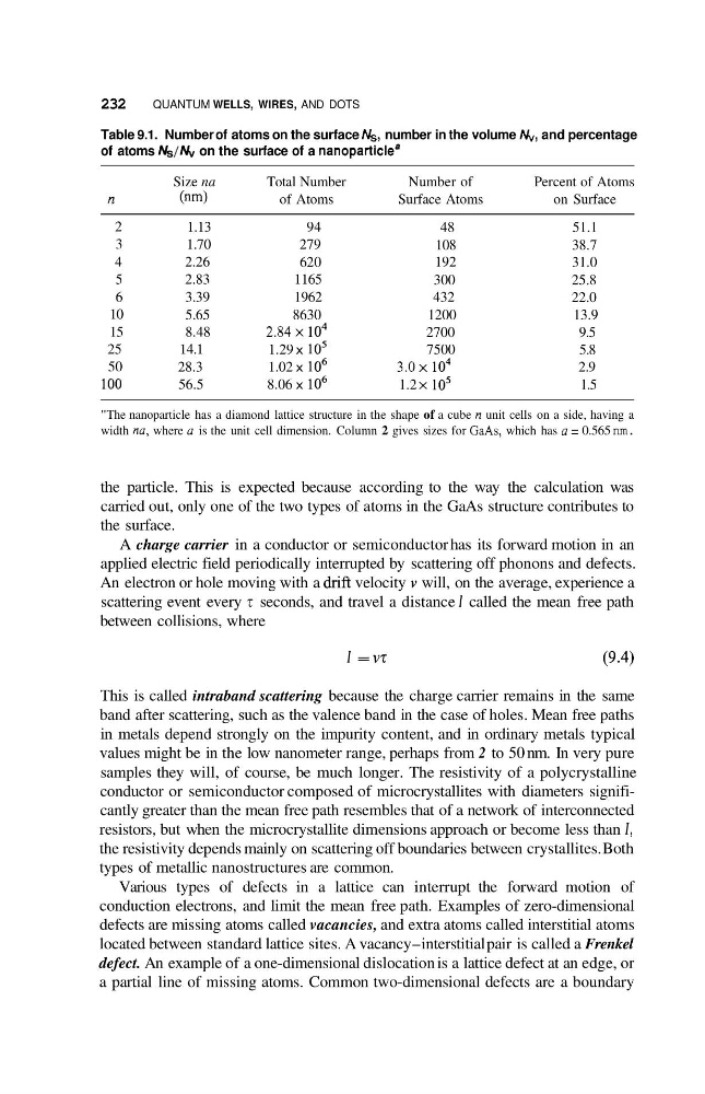
Table 9.1. Number of atoms on the surface b&, number in the volume IU,, and percentage
of atoms Ns/IU, on the surface of a nanoparticle*
Size na
Total Number
Number of
Percent of Atoms
n
(nm)
of Atoms
Surface Atoms
on Surface
2
3
4
5
6
10
15
25
50
I00
1.13
1.70
2.26
2.83
3.39
5.65
8.48
14.1
28.3
56.5
94
279
62 0
1165
1962
8630
2.84 io4
1.02 x lo6
1.29 x lo5
8.06 x lo6
48
108
192
300
432
1200
2700
7500
3.0 io4
1.2 io5
51.1
38.7
31.0
25.8
22.0
13.9
9.5
5.8
2.9
1.5
"The nanoparticle has a diamond lattice structure in the shape of a cube n unit cells on a side, having a
width nu, where u is the unit cell dimension. Column 2 gives sizes for GaAs, which has u = 0.565 nm.
the particle. This is expected because according to the way the calculation was
carried out, only one of the two types of atoms in the GaAs structure contributes to
the surface.
A charge carrier in a conductor or semiconductor has its forward motion in an
applied electric field periodically interrupted by scattering off phonons and defects.
An electron or hole moving with a dnft velocity v will, on the average, experience a
scattering event every z seconds, and travel a distance I called the mean free path
between collisions, where
I = vz
(9.4)
This is called intraband scattering because the charge carrier remains in the same
band after scattering, such as the valence band in the case of holes. Mean free paths
in metals depend strongly on the impurity content, and in ordinary metals typical
values might be in the low nanometer range, perhaps from 2 to 50 nm. In very pure
samples they will, of course, be much longer. The resistivity of a polycrystalline
conductor or semiconductor composed of microcrystallites with diameters significantly greater than the mean free path resembles that of a network of interconnected
resistors, but when the microcrystallite dimensions approach or become less than I,
the resistivity depends mainly on scattering off boundaries between crystallites. Both
types of metallic nanostructures are common.
Various types of defects in a lattice can interrupt the forward motion of
conduction electrons, and limit the mean free path. Examples of zero-dimensional
defects are missing atoms called vacancies, and extra atoms called interstitial atoms
located between standard lattice sites. A vacancy-interstitial pair is called a Frenkel
defect. An example of a one-dimensional dislocation is a lattice defect at an edge, or
a partial line of missing atoms. Common two-dimensional defects are a boundary
QUANTUM WELLS, WIRES, AND DOTS
Table 9.1. Number of atoms on the surface b&, number in the volume IU,, and percentage
of atoms Ns/IU, on the surface of a nanoparticle*
Size na
Total Number
Number of
Percent of Atoms
n
(nm)
of Atoms
Surface Atoms
on Surface
2
3
4
5
6
10
15
25
50
I00
1.13
1.70
2.26
2.83
3.39
5.65
8.48
14.1
28.3
56.5
94
279
62 0
1165
1962
8630
2.84 io4
1.02 x lo6
1.29 x lo5
8.06 x lo6
48
108
192
300
432
1200
2700
7500
3.0 io4
1.2 io5
51.1
38.7
31.0
25.8
22.0
13.9
9.5
5.8
2.9
1.5
"The nanoparticle has a diamond lattice structure in the shape of a cube n unit cells on a side, having a
width nu, where u is the unit cell dimension. Column 2 gives sizes for GaAs, which has u = 0.565 nm.
the particle. This is expected because according to the way the calculation was
carried out, only one of the two types of atoms in the GaAs structure contributes to
the surface.
A charge carrier in a conductor or semiconductor has its forward motion in an
applied electric field periodically interrupted by scattering off phonons and defects.
An electron or hole moving with a dnft velocity v will, on the average, experience a
scattering event every z seconds, and travel a distance I called the mean free path
between collisions, where
I = vz
(9.4)
This is called intraband scattering because the charge carrier remains in the same
band after scattering, such as the valence band in the case of holes. Mean free paths
in metals depend strongly on the impurity content, and in ordinary metals typical
values might be in the low nanometer range, perhaps from 2 to 50 nm. In very pure
samples they will, of course, be much longer. The resistivity of a polycrystalline
conductor or semiconductor composed of microcrystallites with diameters significantly greater than the mean free path resembles that of a network of interconnected
resistors, but when the microcrystallite dimensions approach or become less than I,
the resistivity depends mainly on scattering off boundaries between crystallites. Both
types of metallic nanostructures are common.
Various types of defects in a lattice can interrupt the forward motion of
conduction electrons, and limit the mean free path. Examples of zero-dimensional
defects are missing atoms called vacancies, and extra atoms called interstitial atoms
located between standard lattice sites. A vacancy-interstitial pair is called a Frenkel
defect. An example of a one-dimensional dislocation is a lattice defect at an edge, or
a partial line of missing atoms. Common two-dimensional defects are a boundary