

9.3. SIZE AND DIMENSIONALITY EFFECTS
231
3-nm-thick layers of Si and Sio,7Geo.3 patterned into quantum-dot arrays consisting
of 300-nm-high columns with 60 nm diameters and 200 nm separations.
9.3. SIZE AND DIMENSIONALITY EFFECTS
9.3.1. Size Effects
Now that we have seen how to make nanostructures, it is appropriate to say
something about their sizes relative to various parameters of the system. If we
select the type III-V semiconductor GaAs as a typical material, the lattice constant
from Table B. 1 (of Appendix B) is a = 0.565 nm, and the volume of the unit cell is
(0.565p = 0.180nm’. The unit cell contains four Ga and four As atoms. Each of
these atoms lies on a face-centered cubic (FCC) lattice, shown sketched in Fig. 2.3,
and the two lattices are displaced with respect to each other by the amount i 4 i
along the unit cell body diagonal, as shown in Fig. 2.8. This puts each Ga atom in
the center of a tetrahedron of As atoms corresponding to the grouping GaAs,, and
each arsenic atom has a corresponding configuration AsGa,. There are about 22 of
each atom type per cubic nanometer, and a cube-shaped quantum dot lOnm on a
side contains 5.56 x lo3 unit cells.
The question arises as to how many of the atoms are on the surface, and it will be
helpfd to have a mathematical expression for this in terms of the size of a particle
with the zinc blende structure of GaAs, which has the shape of a cube. If the initial
cube is taken in the form of Fig. 2.6 and nanostructures containing n3 of these unit
cells are built up, then it can be shown that the number of atoms N , on the surface,
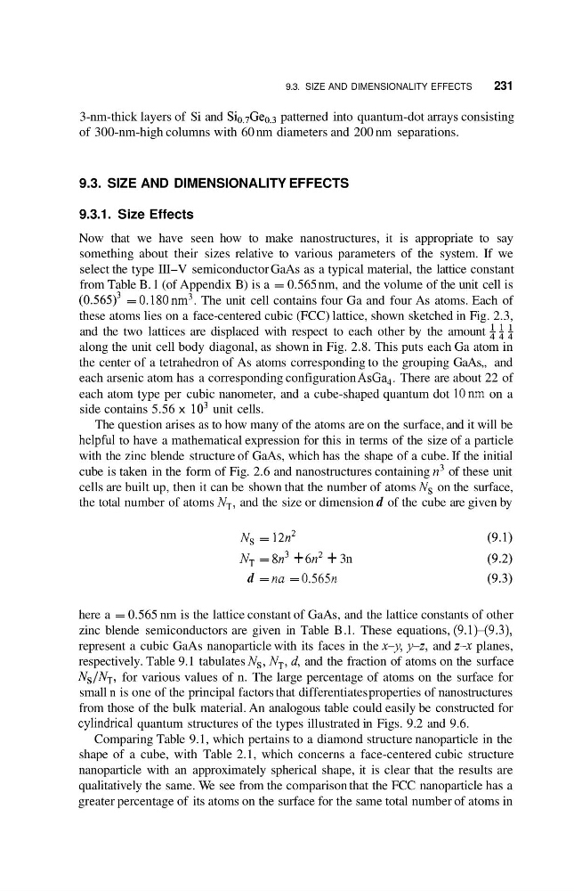
the total number of atoms NT, and the size or dimension d of the cube are given by
N, = 12n2
NT = 8n3 + 6n2 + 3n
d = nu = 0.565n
here a = 0.565 nm is the lattice constant of GaAs, and the lattice constants of other
zinc blende semiconductors are given in Table B.l. These equations, (9.1H9.3),
represent a cubic GaAs nanoparticle with its faces in the x-y, y-z, and z-x planes,
respectively. Table 9.1 tabulates N,, NT, d, and the fraction of atoms on the surface
Ns/NT, for various values of n. The large percentage of atoms on the surface for
small n is one of the principal factors that differentiates properties of nanostructures
from those of the bulk material. An analogous table could easily be constructed for
cylindncal quantum structures of the types illustrated in Figs. 9.2 and 9.6.
Comparing Table 9.1, which pertains to a diamond structure nanoparticle in the
shape of a cube, with Table 2.1, which concerns a face-centered cubic structure
nanoparticle with an approximately spherical shape, it is clear that the results are
qualitatively the same. We see from the comparison that the FCC nanoparticle has a
greater percentage of its atoms on the surface for the same total number of atoms in
231
3-nm-thick layers of Si and Sio,7Geo.3 patterned into quantum-dot arrays consisting
of 300-nm-high columns with 60 nm diameters and 200 nm separations.
9.3. SIZE AND DIMENSIONALITY EFFECTS
9.3.1. Size Effects
Now that we have seen how to make nanostructures, it is appropriate to say
something about their sizes relative to various parameters of the system. If we
select the type III-V semiconductor GaAs as a typical material, the lattice constant
from Table B. 1 (of Appendix B) is a = 0.565 nm, and the volume of the unit cell is
(0.565p = 0.180nm’. The unit cell contains four Ga and four As atoms. Each of
these atoms lies on a face-centered cubic (FCC) lattice, shown sketched in Fig. 2.3,
and the two lattices are displaced with respect to each other by the amount i 4 i
along the unit cell body diagonal, as shown in Fig. 2.8. This puts each Ga atom in
the center of a tetrahedron of As atoms corresponding to the grouping GaAs,, and
each arsenic atom has a corresponding configuration AsGa,. There are about 22 of
each atom type per cubic nanometer, and a cube-shaped quantum dot lOnm on a
side contains 5.56 x lo3 unit cells.
The question arises as to how many of the atoms are on the surface, and it will be
helpfd to have a mathematical expression for this in terms of the size of a particle
with the zinc blende structure of GaAs, which has the shape of a cube. If the initial
cube is taken in the form of Fig. 2.6 and nanostructures containing n3 of these unit
cells are built up, then it can be shown that the number of atoms N , on the surface,
the total number of atoms NT, and the size or dimension d of the cube are given by
N, = 12n2
NT = 8n3 + 6n2 + 3n
d = nu = 0.565n
here a = 0.565 nm is the lattice constant of GaAs, and the lattice constants of other
zinc blende semiconductors are given in Table B.l. These equations, (9.1H9.3),
represent a cubic GaAs nanoparticle with its faces in the x-y, y-z, and z-x planes,
respectively. Table 9.1 tabulates N,, NT, d, and the fraction of atoms on the surface
Ns/NT, for various values of n. The large percentage of atoms on the surface for
small n is one of the principal factors that differentiates properties of nanostructures
from those of the bulk material. An analogous table could easily be constructed for
cylindncal quantum structures of the types illustrated in Figs. 9.2 and 9.6.
Comparing Table 9.1, which pertains to a diamond structure nanoparticle in the
shape of a cube, with Table 2.1, which concerns a face-centered cubic structure
nanoparticle with an approximately spherical shape, it is clear that the results are
qualitatively the same. We see from the comparison that the FCC nanoparticle has a
greater percentage of its atoms on the surface for the same total number of atoms in