

9.2. PREPARATION OF QUANTUM NANOSTRUCTURES
229
i
The first step of the lithographic procedure is to place a radiation-sensitive resist
on the surface of the sample substrate, as shown in Fig. 9.4a. The sample is then
irradiated by an electron beam in the region where the nanostructure will be located,
as shown in Fig. 9.4b. This can be done by using either a radiation mask that
contains the nanostructure pattern, as shown, or a scanning electron beam that strikes
the surface only in the desired region. The radiation chemically modifies the exposed
area of the resist so that it becomes soluble in a developer. The third step in the
process (Fig. 9 . 4 ~ ) is the application of the developer to remove the irradiated
portions of the resist. The fourth step (Fig. 9.4d) is the insertion of an etching mask
into the hole in the resist, and the fifth step (Fig. 9.4e) consists in lifting off the
remaining parts of the resist. In the sixth step (Fig. 9.40 the areas of the quantum
well not covered by the etching mask are chemically etched away to produce the
quantum structure shown in Fig. 9.4f covered by the etching mask. Finally the
etching mask is removed, if necessary, to provide the desired quantum structure
(Fig. 9.4g), which might be the quantum wire or quantum dot shown in Fig. 9.3b.
In Chapter 1 we mentioned the most common process called electron-beam
lithography, which makes use of an electron beam for the radiation. Other types of
lithography employ neutral atom beams (e.g., Li, Na, K, Rb, Cs), charged ion beams
(e.g., Gaf), or electromagnetic radiation such as visible light, ultraviolet light, or X
rays. When laser beams are utilized, frequency doublers and quadruplers can bring the
wavelength into a range (e.g., A- 150nm) that is convenient for quantum-dot
fabrication. Photochemical etching can be applied to a surface activated by laser light.
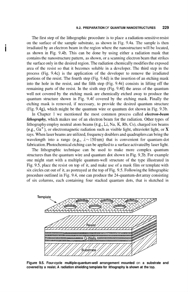
The lithographic technique can be used to make more complex quantum
structures than the quantum wire and quantum dot shown in Fig. 9.3b. For example
one might start with a multiple quantum-well structure of the type illustrated in
Fig. 9.5, place the resist on top of it, and make use of a mask film or template with
six circles cut out of it, as portrayed at the top of Fig. 9.5. Following the lithographic
procedure outlined in Fig. 9.4, one can produce the 24-quantum-dot array consisting
of six columns, each containing four stacked quantum dots, that is sketched in
Figure 9.5. Four-cycle multiple-quantum-well arrangement mounted on a substrate and
covered by a resist. A radiation shielding template for lithography is shown at the top.
229
i
The first step of the lithographic procedure is to place a radiation-sensitive resist
on the surface of the sample substrate, as shown in Fig. 9.4a. The sample is then
irradiated by an electron beam in the region where the nanostructure will be located,
as shown in Fig. 9.4b. This can be done by using either a radiation mask that
contains the nanostructure pattern, as shown, or a scanning electron beam that strikes
the surface only in the desired region. The radiation chemically modifies the exposed
area of the resist so that it becomes soluble in a developer. The third step in the
process (Fig. 9 . 4 ~ ) is the application of the developer to remove the irradiated
portions of the resist. The fourth step (Fig. 9.4d) is the insertion of an etching mask
into the hole in the resist, and the fifth step (Fig. 9.4e) consists in lifting off the
remaining parts of the resist. In the sixth step (Fig. 9.40 the areas of the quantum
well not covered by the etching mask are chemically etched away to produce the
quantum structure shown in Fig. 9.4f covered by the etching mask. Finally the
etching mask is removed, if necessary, to provide the desired quantum structure
(Fig. 9.4g), which might be the quantum wire or quantum dot shown in Fig. 9.3b.
In Chapter 1 we mentioned the most common process called electron-beam
lithography, which makes use of an electron beam for the radiation. Other types of
lithography employ neutral atom beams (e.g., Li, Na, K, Rb, Cs), charged ion beams
(e.g., Gaf), or electromagnetic radiation such as visible light, ultraviolet light, or X
rays. When laser beams are utilized, frequency doublers and quadruplers can bring the
wavelength into a range (e.g., A- 150nm) that is convenient for quantum-dot
fabrication. Photochemical etching can be applied to a surface activated by laser light.
The lithographic technique can be used to make more complex quantum
structures than the quantum wire and quantum dot shown in Fig. 9.3b. For example
one might start with a multiple quantum-well structure of the type illustrated in
Fig. 9.5, place the resist on top of it, and make use of a mask film or template with
six circles cut out of it, as portrayed at the top of Fig. 9.5. Following the lithographic
procedure outlined in Fig. 9.4, one can produce the 24-quantum-dot array consisting
of six columns, each containing four stacked quantum dots, that is sketched in
Figure 9.5. Four-cycle multiple-quantum-well arrangement mounted on a substrate and
covered by a resist. A radiation shielding template for lithography is shown at the top.