

228
QUANTUM WELLS, WIRES, AND DOTS
Wire
f 3 7
Substrate
! ?7 Substrate
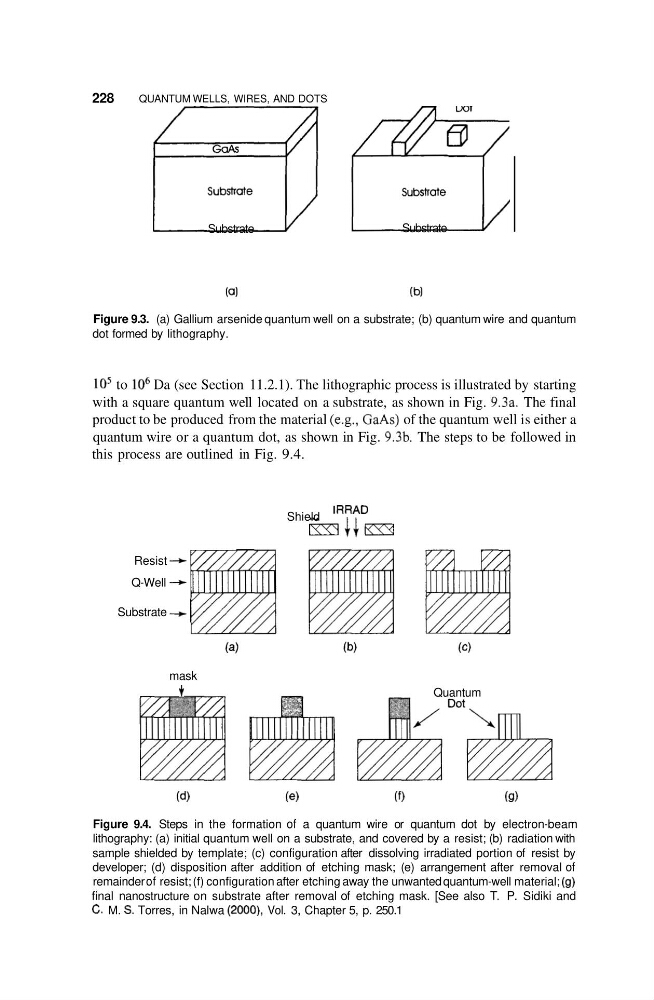
Figure 9.3. (a) Gallium arsenide quantum well on a substrate; (b) quantum wire and quantum
dot formed by lithography.
lo5 to lo6 Da (see Section 11.2.1). The lithographic process is illustrated by starting
with a square quantum well located on a substrate, as shown in Fig. 9.3a. The final
product to be produced from the material (e.g., GaAs) of the quantum well is either a
quantum wire or a quantum dot, as shown in Fig. 9.3b. The steps to be followed in
this process are outlined in Fig. 9.4.
IRRAD
Shield
m c c m
Resist -+
Q-Well -+
Substrate -+
mask
t
Quantum
( 4
(e)
(f)
(9)
Figure 9.4. Steps in the formation of a quantum wire or quantum dot by electron-beam
lithography: (a) initial quantum well on a substrate, and covered by a resist; (b) radiation with
sample shielded by template; (c) configuration after dissolving irradiated portion of resist by
developer; (d) disposition after addition of etching mask; (e) arrangement after removal of
remainder of resist; (f) configuration after etching away the unwanted quantum-well material; (9)
final nanostructure on substrate after removal of etching mask. [See also T. P. Sidiki and
C. M. S. Torres, in Nalwa (2000), Vol. 3, Chapter 5, p. 250.1
QUANTUM WELLS, WIRES, AND DOTS
Wire
f 3 7
Substrate
! ?7 Substrate
Figure 9.3. (a) Gallium arsenide quantum well on a substrate; (b) quantum wire and quantum
dot formed by lithography.
lo5 to lo6 Da (see Section 11.2.1). The lithographic process is illustrated by starting
with a square quantum well located on a substrate, as shown in Fig. 9.3a. The final
product to be produced from the material (e.g., GaAs) of the quantum well is either a
quantum wire or a quantum dot, as shown in Fig. 9.3b. The steps to be followed in
this process are outlined in Fig. 9.4.
IRRAD
Shield
m c c m
Resist -+
Q-Well -+
Substrate -+
mask
t
Quantum
( 4
(e)
(f)
(9)
Figure 9.4. Steps in the formation of a quantum wire or quantum dot by electron-beam
lithography: (a) initial quantum well on a substrate, and covered by a resist; (b) radiation with
sample shielded by template; (c) configuration after dissolving irradiated portion of resist by
developer; (d) disposition after addition of etching mask; (e) arrangement after removal of
remainder of resist; (f) configuration after etching away the unwanted quantum-well material; (9)
final nanostructure on substrate after removal of etching mask. [See also T. P. Sidiki and
C. M. S. Torres, in Nalwa (2000), Vol. 3, Chapter 5, p. 250.1