

162
BULK NANOSTRUCTURED MATERIALS
0
3
$ 0.3
Z 0.4 ~ T M
PHOTONIC BAND GAP:
1
-
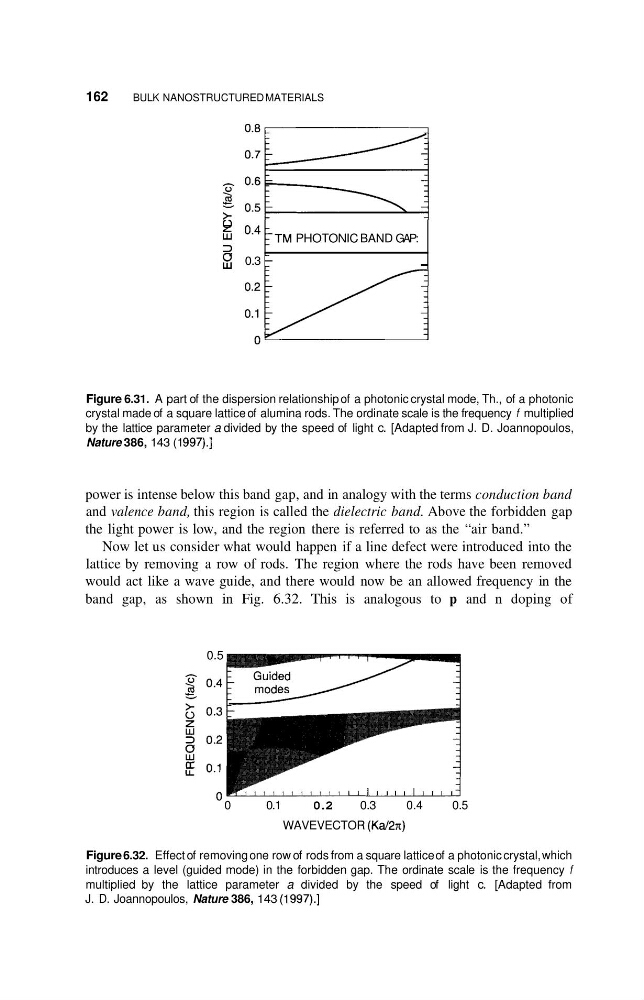
Figure 6.31. A part of the dispersion relationship of a photonic crystal mode, Th., of a photonic
crystal made of a square lattice of alumina rods. The ordinate scale is the frequency f multiplied
by the lattice parameter a divided by the speed of light c. [Adapted from J. D. Joannopoulos,
Nature 386, 143 (1 997).]
power is intense below this band gap, and in analogy with the terms conduction band
and valence band, this region is called the dielectric band. Above the forbidden gap
the light power is low, and the region there is referred to as the “air band.”
Now let us consider what would happen if a line defect were introduced into the
lattice by removing a row of rods. The region where the rods have been removed
would act like a wave guide, and there would now be an allowed frequency in the
band gap, as shown in Fig. 6.32. This is analogous to p and n doping of
0.5
c1 1 1 1 1 1 1 1 1 1 1 I l l , I I I l l , , I
0
0.1
0.2
0.3
0.4
0.5
WAVEVECTOR (Ka/2n)
Figure 6.32. Effect of removing one row of rods from a square lattice of a photonic crystal, which
introduces a level (guided mode) in the forbidden gap. The ordinate scale is the frequency f
multiplied by the lattice parameter a divided by the speed of light c. [Adapted from
J. D. Joannopoulos, Nature 386, 143 (1997).]
BULK NANOSTRUCTURED MATERIALS
0
3
$ 0.3
Z 0.4 ~ T M
PHOTONIC BAND GAP:
1
-
Figure 6.31. A part of the dispersion relationship of a photonic crystal mode, Th., of a photonic
crystal made of a square lattice of alumina rods. The ordinate scale is the frequency f multiplied
by the lattice parameter a divided by the speed of light c. [Adapted from J. D. Joannopoulos,
Nature 386, 143 (1 997).]
power is intense below this band gap, and in analogy with the terms conduction band
and valence band, this region is called the dielectric band. Above the forbidden gap
the light power is low, and the region there is referred to as the “air band.”
Now let us consider what would happen if a line defect were introduced into the
lattice by removing a row of rods. The region where the rods have been removed
would act like a wave guide, and there would now be an allowed frequency in the
band gap, as shown in Fig. 6.32. This is analogous to p and n doping of
0.5
c1 1 1 1 1 1 1 1 1 1 1 I l l , I I I l l , , I
0
0.1
0.2
0.3
0.4
0.5
WAVEVECTOR (Ka/2n)
Figure 6.32. Effect of removing one row of rods from a square lattice of a photonic crystal, which
introduces a level (guided mode) in the forbidden gap. The ordinate scale is the frequency f
multiplied by the lattice parameter a divided by the speed of light c. [Adapted from
J. D. Joannopoulos, Nature 386, 143 (1997).]