

160
BULK NANOSTRUCTURED MATERIALS
where Vis the volume of the solid, the momentum p = Ak, and the wavevector k is
related to the wavelength A by the expression k = 271/2. In the nearly free-electron
model of metals the valence or conduction electrons are treated as noninteracting
free electrons moving in a periodic potential arising from the positively charged ion
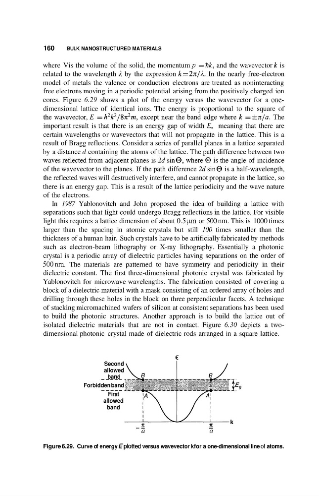
cores. Figure 6.29 shows a plot of the energy versus the wavevector for a onedimensional lattice of identical ions. The energy is proportional to the square of
the wavevector, E = h2k2/8n2m, except near the band edge where k = frc/a. The
important result is that there is an energy gap of width E,, meaning that there are
certain wavelengths or wavevectors that will not propagate in the lattice. This is a
result of Bragg reflections. Consider a series of parallel planes in a lattice separated
by a distance d containing the atoms of the lattice. The path difference between two
waves reflected from adjacent planes is 2d sin 0, where 0 is the angle of incidence
of the wavevector to the planes. If the path difference 2d sin 0 is a half-wavelength,
the reflected waves will destructively interfere, and cannot propagate in the lattice, so
there is an energy gap. This is a result of the lattice periodicity and the wave nature
of the electrons.
In 1987 Yablonovitch and John proposed the idea of building a lattice with
separations such that light could undergo Bragg reflections in the lattice. For visible
light this requires a lattice dimension of about 0.5 pm or 500 nm. This is 1000 times
larger than the spacing in atomic crystals but still 100 times smaller than the
thickness of a human hair. Such crystals have to be artificially fabricated by methods
such as electron-beam lithography or X-ray lithography. Essentially a photonic
crystal is a periodic array of dielectric particles having separations on the order of
500nm. The materials are patterned to have symmetry and periodicity in their
dielectric constant. The first three-dimensional photonic crystal was fabricated by
Yablonovitch for microwave wavelengths. The fabrication consisted of covering a
block of a dielectric material with a mask consisting of an ordered array of holes and
drilling through these holes in the block on three perpendicular facets. A technique
of stacking micromachined wafers of silicon at consistent separations has been used
to build the photonic structures. Another approach is to build the lattice out of
isolated dielectric materials that are not in contact. Figure 6.30 depicts a twodimensional photonic crystal made of dielectric rods arranged in a square lattice.
€
Second
allowed
band
Forbidden band
First
allowed
band
_ _ _ _ -
- _ _ _ _
x
x
k
- _
-
a
a
Figure 6.29. Curve of energy €plotted versus wavevector kfor a one-dimensional line of atoms.
BULK NANOSTRUCTURED MATERIALS
where Vis the volume of the solid, the momentum p = Ak, and the wavevector k is
related to the wavelength A by the expression k = 271/2. In the nearly free-electron
model of metals the valence or conduction electrons are treated as noninteracting
free electrons moving in a periodic potential arising from the positively charged ion
cores. Figure 6.29 shows a plot of the energy versus the wavevector for a onedimensional lattice of identical ions. The energy is proportional to the square of
the wavevector, E = h2k2/8n2m, except near the band edge where k = frc/a. The
important result is that there is an energy gap of width E,, meaning that there are
certain wavelengths or wavevectors that will not propagate in the lattice. This is a
result of Bragg reflections. Consider a series of parallel planes in a lattice separated
by a distance d containing the atoms of the lattice. The path difference between two
waves reflected from adjacent planes is 2d sin 0, where 0 is the angle of incidence
of the wavevector to the planes. If the path difference 2d sin 0 is a half-wavelength,
the reflected waves will destructively interfere, and cannot propagate in the lattice, so
there is an energy gap. This is a result of the lattice periodicity and the wave nature
of the electrons.
In 1987 Yablonovitch and John proposed the idea of building a lattice with
separations such that light could undergo Bragg reflections in the lattice. For visible
light this requires a lattice dimension of about 0.5 pm or 500 nm. This is 1000 times
larger than the spacing in atomic crystals but still 100 times smaller than the
thickness of a human hair. Such crystals have to be artificially fabricated by methods
such as electron-beam lithography or X-ray lithography. Essentially a photonic
crystal is a periodic array of dielectric particles having separations on the order of
500nm. The materials are patterned to have symmetry and periodicity in their
dielectric constant. The first three-dimensional photonic crystal was fabricated by
Yablonovitch for microwave wavelengths. The fabrication consisted of covering a
block of a dielectric material with a mask consisting of an ordered array of holes and
drilling through these holes in the block on three perpendicular facets. A technique
of stacking micromachined wafers of silicon at consistent separations has been used
to build the photonic structures. Another approach is to build the lattice out of
isolated dielectric materials that are not in contact. Figure 6.30 depicts a twodimensional photonic crystal made of dielectric rods arranged in a square lattice.
€
Second
allowed
band
Forbidden band
First
allowed
band
_ _ _ _ -
- _ _ _ _
x
x
k
- _
-
a
a
Figure 6.29. Curve of energy €plotted versus wavevector kfor a one-dimensional line of atoms.