

150
BULK NANOSTRUCTURED MATERIALS
V, battery
I
salt bath
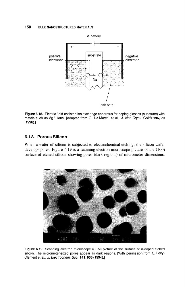
Figure 6.18. Electric field assisted ion exchange apparatus for doping glasses (substrate) with
metals such as Ag+ ions. [Adapted from G. De Marchi et al., J. Non-Cryst. Solids 196, 79
(1 996).]
6.1.8. Porous Silicon
When a wafer of silicon is subjected to electrochemical etching, the silicon wafer
develops pores. Figure 6.19 is a scanning electron microscope picture of the (100)
surface of etched silicon showing pores (dark regions) of micrometer dimensions.
Figure 6.19. Scanning electron microscope (SEM) picture of the surface of n-doped etched
silicon. The micrometer-sized pores appear as dark regions. [With permission from C. LevyClement et al., J. Electrochem. Soc. 141, 958 (1994).]
BULK NANOSTRUCTURED MATERIALS
V, battery
I
salt bath
Figure 6.18. Electric field assisted ion exchange apparatus for doping glasses (substrate) with
metals such as Ag+ ions. [Adapted from G. De Marchi et al., J. Non-Cryst. Solids 196, 79
(1 996).]
6.1.8. Porous Silicon
When a wafer of silicon is subjected to electrochemical etching, the silicon wafer
develops pores. Figure 6.19 is a scanning electron microscope picture of the (100)
surface of etched silicon showing pores (dark regions) of micrometer dimensions.
Figure 6.19. Scanning electron microscope (SEM) picture of the surface of n-doped etched
silicon. The micrometer-sized pores appear as dark regions. [With permission from C. LevyClement et al., J. Electrochem. Soc. 141, 958 (1994).]