

142
BULK NANOSTRUCTURED MATERIALS
39 7
37 7
m
h
a"
v (3 35:
w 33:
3 1 1
29 :
0
0
Z
I
m
2 5 F " 1 ' ' " " 1 1 " " 1 ' 1 1 "
0
50
100 150 200 250 300
BILAYER PERIOD (nm)
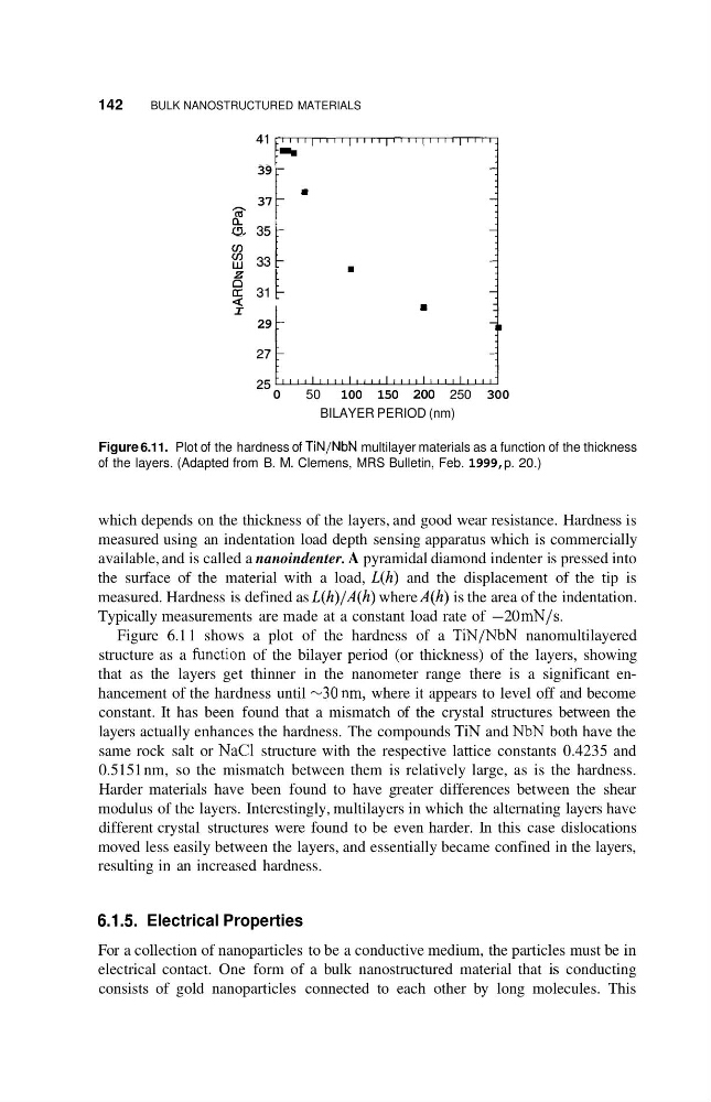
Figure 6.11. Plot of the hardness of TiN/NbN multilayer materials as a function of the thickness
of the layers. (Adapted from B. M. Clemens, MRS Bulletin, Feb. 1999, p. 20.)
which depends on the thickness of the layers, and good wear resistance. Hardness is
measured using an indentation load depth sensing apparatus which is commercially
available, and is called a nanoindenter. A pyramidal diamond indenter is pressed into
the surface of the material with a load, L(h) and the displacement of the tip is
measured. Hardness is defined as L(h)/A(h) where A(h) is the area of the indentation.
Typically measurements are made at a constant load rate of -20 mN/s.
Figure 6.1 1 shows a plot of the hardness of a TiN/NbN nanomultilayered
structure as a fimction of the bilayer period (or thickness) of the layers, showing
that as the layers get thinner in the nanometer range there is a significant enhancement of the hardness until -30nm, where it appears to level off and become
constant. It has been found that a mismatch of the crystal structures between the
layers actually enhances the hardness. The compounds TIN and NbN both have the
same rock salt or NaCl structure with the respective lattice constants 0.4235 and
0.5151 nm, so the mismatch between them is relatively large, as is the hardness.
Harder materials have been found to have greater differences between the shear
modulus of the layers. Interestingly, multilayers in which the alternating layers have
different crystal structures were found to be even harder. In this case dislocations
moved less easily between the layers, and essentially became confined in the layers,
resulting in an increased hardness.
6.1.5. Electrical Properties
For a collection of nanoparticles to be a conductive medium, the particles must be in
electrical contact. One form of a bulk nanostructured material that is conducting
consists of gold nanoparticles connected to each other by long molecules. This
BULK NANOSTRUCTURED MATERIALS
39 7
37 7
m
h
a"
v (3 35:
w 33:
3 1 1
29 :
0
0
Z
I
m
2 5 F " 1 ' ' " " 1 1 " " 1 ' 1 1 "
0
50
100 150 200 250 300
BILAYER PERIOD (nm)
Figure 6.11. Plot of the hardness of TiN/NbN multilayer materials as a function of the thickness
of the layers. (Adapted from B. M. Clemens, MRS Bulletin, Feb. 1999, p. 20.)
which depends on the thickness of the layers, and good wear resistance. Hardness is
measured using an indentation load depth sensing apparatus which is commercially
available, and is called a nanoindenter. A pyramidal diamond indenter is pressed into
the surface of the material with a load, L(h) and the displacement of the tip is
measured. Hardness is defined as L(h)/A(h) where A(h) is the area of the indentation.
Typically measurements are made at a constant load rate of -20 mN/s.
Figure 6.1 1 shows a plot of the hardness of a TiN/NbN nanomultilayered
structure as a fimction of the bilayer period (or thickness) of the layers, showing
that as the layers get thinner in the nanometer range there is a significant enhancement of the hardness until -30nm, where it appears to level off and become
constant. It has been found that a mismatch of the crystal structures between the
layers actually enhances the hardness. The compounds TIN and NbN both have the
same rock salt or NaCl structure with the respective lattice constants 0.4235 and
0.5151 nm, so the mismatch between them is relatively large, as is the hardness.
Harder materials have been found to have greater differences between the shear
modulus of the layers. Interestingly, multilayers in which the alternating layers have
different crystal structures were found to be even harder. In this case dislocations
moved less easily between the layers, and essentially became confined in the layers,
resulting in an increased hardness.
6.1.5. Electrical Properties
For a collection of nanoparticles to be a conductive medium, the particles must be in
electrical contact. One form of a bulk nanostructured material that is conducting
consists of gold nanoparticles connected to each other by long molecules. This