

6.1. SOLID DISORDERED NANOSTRUCTURES
141
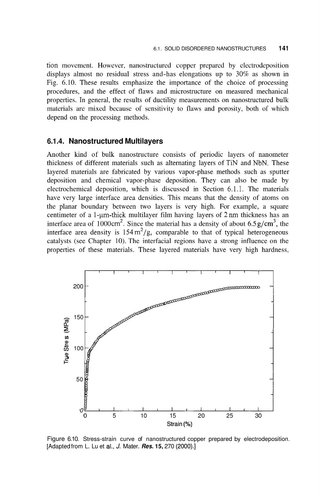
tion movement. However, nanostructured copper prepared by electrodeposition
displays almost no residual stress and-has elongations up to 30% as shown in
Fig. 6.10. These results emphasize the importance of the choice of processing
procedures, and the effect of flaws and microstructure on measured mechanical
properties. In general, the results of ductility measurements on nanostructured bulk
materials are mixed because of sensitivity to flaws and porosity, both of which
depend on the processing methods.
6.1.4. Nanostructured Multilayers
Another kind of bulk nanostructure consists of periodic layers of nanometer
thickness of different materials such as alternating layers of TiN and NbN. These
layered materials are fabricated by various vapor-phase methods such as sputter
deposition and chemical vapor-phase deposition. They can also be made by
electrochemical deposition, which is discussed in Section 6.1.1. The materials
have very large interface area densities. This means that the density of atoms on
the planar boundary between two layers is very high. For example, a square
centimeter of a 1-pm-thick multilayer film having layers of 2nm thickness has an
interface area of 1000 cm2. Since the material has a density of about 6.5 g/cm3, the
interface area density is 154m2/g, comparable to that of typical heterogeneous
catalysts (see Chapter 10). The interfacial regions have a strong influence on the
properties of these materials. These layered materials have very high hardness,
200
- 150
2
v) v)
5 100
3
50
0
0
5
10
15
20
25
30
Strain (Yo)
Strain (Yo)
Figure 6.10. Stress-strain curve of nanostructured copper prepared by electrodeposition.
[Adapted from L. Lu et al., J. Mater. Res. 15, 270 (2000).]
141
tion movement. However, nanostructured copper prepared by electrodeposition
displays almost no residual stress and-has elongations up to 30% as shown in
Fig. 6.10. These results emphasize the importance of the choice of processing
procedures, and the effect of flaws and microstructure on measured mechanical
properties. In general, the results of ductility measurements on nanostructured bulk
materials are mixed because of sensitivity to flaws and porosity, both of which
depend on the processing methods.
6.1.4. Nanostructured Multilayers
Another kind of bulk nanostructure consists of periodic layers of nanometer
thickness of different materials such as alternating layers of TiN and NbN. These
layered materials are fabricated by various vapor-phase methods such as sputter
deposition and chemical vapor-phase deposition. They can also be made by
electrochemical deposition, which is discussed in Section 6.1.1. The materials
have very large interface area densities. This means that the density of atoms on
the planar boundary between two layers is very high. For example, a square
centimeter of a 1-pm-thick multilayer film having layers of 2nm thickness has an
interface area of 1000 cm2. Since the material has a density of about 6.5 g/cm3, the
interface area density is 154m2/g, comparable to that of typical heterogeneous
catalysts (see Chapter 10). The interfacial regions have a strong influence on the
properties of these materials. These layered materials have very high hardness,
200
- 150
2
v) v)
5 100
3
50
0
0
5
10
15
20
25
30
Strain (Yo)
Strain (Yo)
Figure 6.10. Stress-strain curve of nanostructured copper prepared by electrodeposition.
[Adapted from L. Lu et al., J. Mater. Res. 15, 270 (2000).]