

5.4. CARBON NANOTUBES
11 9
investigate the electronic structure of carbon nanotubes. In this measurement the
position of the STM tip is fixed above the nanotube, and the voltage V between the
tip and the sample is swept while the tunneling current Z is monitored. The measured
conductance G = I / Vis a direct measure of the local electronic density of states. The
density of states, discussed in more detail in Chapter 2, is a measure of how close
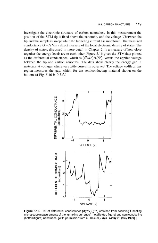
together the energy levels are to each other. Figure 5.16 gives the STM data plotted
as the differential conductance, which is (dI/dV',)/(I/ V',), versus the applied voltage
between the tip and carbon nanotube. The data show clearly the energy gap in
materials at voltages where very little current is observed. The voltage width of this
region measures the gap, which for the semiconducting material shown on the
bottom of Fig. 5.16 is 0.7 eV
I
I
I
I
I
VOLTAGE (V)
W
0
z
s
VOLTAGE (V)
Figure 5.16. Plot of differential conductance ( d / / d V ) ( / / V ) obtained from scanning tunneling
microscope measurements of the tunneling current of metallic (top figure) and semiconducting
(bottom figure) nanotubes. [With permission from C. Dekker, fhys. Today 22 (May 1999).]
11 9
investigate the electronic structure of carbon nanotubes. In this measurement the
position of the STM tip is fixed above the nanotube, and the voltage V between the
tip and the sample is swept while the tunneling current Z is monitored. The measured
conductance G = I / Vis a direct measure of the local electronic density of states. The
density of states, discussed in more detail in Chapter 2, is a measure of how close
together the energy levels are to each other. Figure 5.16 gives the STM data plotted
as the differential conductance, which is (dI/dV',)/(I/ V',), versus the applied voltage
between the tip and carbon nanotube. The data show clearly the energy gap in
materials at voltages where very little current is observed. The voltage width of this
region measures the gap, which for the semiconducting material shown on the
bottom of Fig. 5.16 is 0.7 eV
I
I
I
I
I
VOLTAGE (V)
W
0
z
s
VOLTAGE (V)
Figure 5.16. Plot of differential conductance ( d / / d V ) ( / / V ) obtained from scanning tunneling
microscope measurements of the tunneling current of metallic (top figure) and semiconducting
(bottom figure) nanotubes. [With permission from C. Dekker, fhys. Today 22 (May 1999).]