

E1C07 09/14/2010
14:43:50 Page 279
a 1-MHz clock would require a maximum time of 12 ms per conversion. But this also reveals the
trade-off between increasing the number of bits to lower quantization error and the resulting
increase in conversion time. Faster clocks enable higher sample rates. Common maximum sample
rates are on the order of 100 kHz to 1 MHz using 12, 16, or 24 bits.
Sources of conversion error originate in the accuracies of the D/A converter and the comparator.
Noise is the principal weakness of this type of converter, particularly at the decision points for the
higher-order bits. The successive approximation process requires that the voltage remain constant
during the conversion process. Because of this, a sample-and-hold circuit (SHC), as introduced in
Chapter 6, is used ahead of the converter input to measure and to hold the input voltage value constant
throughout the duration of the conversion. The SHC also minimizes noise during the conversion.
Ramp (Integrating) Converters
Low-level (<1-mV) measurements often rely on ramp converters for their low-noise features. These
integrating analog-to-digital converters use the voltage level of a linear reference ramp signal to
discern the voltage level of the analog input signal and convert it to its binary equivalent. Principal
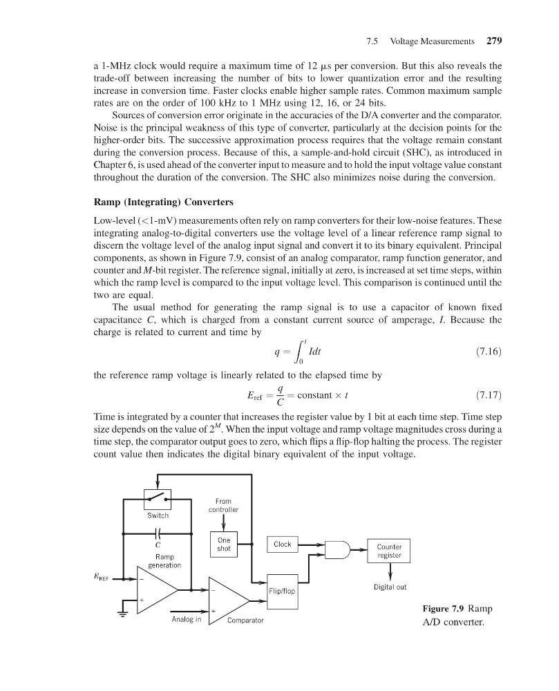
components, as shown in Figure 7.9, consist of an analog comparator, ramp function generator, and
counter and M-bit register. The reference signal, initially at zero, is increased at set time steps, within
which the ramp level is compared to the input voltage level. This comparison is continued until the
two are equal.
The usual method for generating the ramp signal is to use a capacitor of known fixed
capacitance C, which is charged from a constant current source of amperage, I. Because the
charge is related to current and time by
q ¼
Z t
0
Idt
ð7:16Þ
the reference ramp voltage is linearly related to the elapsed time by
E ref ¼
q
C
¼ constant  t
ð7:17Þ
Time is integrated by a counter that increases the register value by 1 bit at each time step. Time step
size depends on the value of 2
M . When the input voltage and ramp voltage magnitudes cross during a
time step, the comparator output goes to zero, which flips a flip-flop halting the process. The register
count value then indicates the digital binary equivalent of the input voltage.
–
+
–
+
From
controller
Switch
Comparator
Analog in
Ramp
generation
C
Digital out
E REF
Clock
Flip/flop
One
shot
Counter
register
Figure 7.9 Ramp
A/D converter.
7.5 Voltage Measurements 279
14:43:50 Page 279
a 1-MHz clock would require a maximum time of 12 ms per conversion. But this also reveals the
trade-off between increasing the number of bits to lower quantization error and the resulting
increase in conversion time. Faster clocks enable higher sample rates. Common maximum sample
rates are on the order of 100 kHz to 1 MHz using 12, 16, or 24 bits.
Sources of conversion error originate in the accuracies of the D/A converter and the comparator.
Noise is the principal weakness of this type of converter, particularly at the decision points for the
higher-order bits. The successive approximation process requires that the voltage remain constant
during the conversion process. Because of this, a sample-and-hold circuit (SHC), as introduced in
Chapter 6, is used ahead of the converter input to measure and to hold the input voltage value constant
throughout the duration of the conversion. The SHC also minimizes noise during the conversion.
Ramp (Integrating) Converters
Low-level (<1-mV) measurements often rely on ramp converters for their low-noise features. These
integrating analog-to-digital converters use the voltage level of a linear reference ramp signal to
discern the voltage level of the analog input signal and convert it to its binary equivalent. Principal
components, as shown in Figure 7.9, consist of an analog comparator, ramp function generator, and
counter and M-bit register. The reference signal, initially at zero, is increased at set time steps, within
which the ramp level is compared to the input voltage level. This comparison is continued until the
two are equal.
The usual method for generating the ramp signal is to use a capacitor of known fixed
capacitance C, which is charged from a constant current source of amperage, I. Because the
charge is related to current and time by
q ¼
Z t
0
Idt
ð7:16Þ
the reference ramp voltage is linearly related to the elapsed time by
E ref ¼
q
C
¼ constant  t
ð7:17Þ
Time is integrated by a counter that increases the register value by 1 bit at each time step. Time step
size depends on the value of 2
M . When the input voltage and ramp voltage magnitudes cross during a
time step, the comparator output goes to zero, which flips a flip-flop halting the process. The register
count value then indicates the digital binary equivalent of the input voltage.
–
+
–
+
From
controller
Switch
Comparator
Analog in
Ramp
generation
C
Digital out
E REF
Clock
Flip/flop
One
shot
Counter
register
Figure 7.9 Ramp
A/D converter.
7.5 Voltage Measurements 279