

E1C07 09/14/2010
14:43:49 Page 278
2. The next highest bit (MSB-1) is set to 1. Again, if E
Ã
> E i , it is reset to 0; otherwise its value
remains 1.
3. The process continues through to the LSB. The final register value gives the quantization
of E i .
The process requires a time of one clock tick per bit.
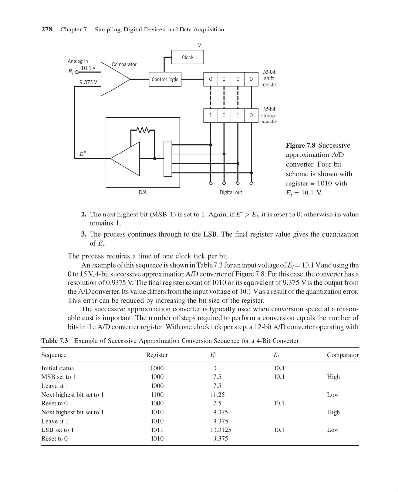
An example of this sequence is shown in Table 7.3 for an input voltage of E i ¼ 10.1 Vand using the
0 to 15 V, 4-bit successive approximation A/D converter of Figure 7.8. For this case, the converter has a
resolution of 0.9375 V. The final register count of 1010 or its equivalent of 9.375 V is the output from
the A/D converter. Its value differs from the input voltage of 10.1 Vas a result of the quantization error.
This error can be reduced by increasing the bit size of the register.
The successive approximation converter is typically used when conversion speed at a reasonable cost is important. The number of steps required to perform a conversion equals the number of
bits in the A/D converter register. With one clock tick per step, a 12-bit A/D converter operating with
Control logic
t
u
o
l
a
t
i
g
i
D
A
/
D
0
0
0
0
1
0
1
0
Analog in
E i
E*
10.1 V
9.375 V
Comparator
M-bit
shift
register
M-bit
storage
register
Clock
V
Figure 7.8 Successive
approximation A/D
converter. Four-bit
scheme is shown with
register = 1010 with
E i = 10.1 V.
Table 7.3 Example of Successive Approximation Conversion Sequence for a 4-Bit Converter
Sequence
Register
E
Ã
E i
Comparator
Initial status
0000
0
10.1
MSB set to 1
1000
7.5
10.1
High
Leave at 1
1000
7.5
Next highest bit set to 1
1100
11.25
Low
Reset to 0
1000
7.5
10.1
Next highest bit set to 1
1010
9.375
High
Leave at 1
1010
9.375
LSB set to 1
1011
10.3125
10.1
Low
Reset to 0
1010
9.375
278 Chapter 7 Sampling, Digital Devices, and Data Acquisition
14:43:49 Page 278
2. The next highest bit (MSB-1) is set to 1. Again, if E
Ã
> E i , it is reset to 0; otherwise its value
remains 1.
3. The process continues through to the LSB. The final register value gives the quantization
of E i .
The process requires a time of one clock tick per bit.
An example of this sequence is shown in Table 7.3 for an input voltage of E i ¼ 10.1 Vand using the
0 to 15 V, 4-bit successive approximation A/D converter of Figure 7.8. For this case, the converter has a
resolution of 0.9375 V. The final register count of 1010 or its equivalent of 9.375 V is the output from
the A/D converter. Its value differs from the input voltage of 10.1 Vas a result of the quantization error.
This error can be reduced by increasing the bit size of the register.
The successive approximation converter is typically used when conversion speed at a reasonable cost is important. The number of steps required to perform a conversion equals the number of
bits in the A/D converter register. With one clock tick per step, a 12-bit A/D converter operating with
Control logic
t
u
o
l
a
t
i
g
i
D
A
/
D
0
0
0
0
1
0
1
0
Analog in
E i
E*
10.1 V
9.375 V
Comparator
M-bit
shift
register
M-bit
storage
register
Clock
V
Figure 7.8 Successive
approximation A/D
converter. Four-bit
scheme is shown with
register = 1010 with
E i = 10.1 V.
Table 7.3 Example of Successive Approximation Conversion Sequence for a 4-Bit Converter
Sequence
Register
E
Ã
E i
Comparator
Initial status
0000
0
10.1
MSB set to 1
1000
7.5
10.1
High
Leave at 1
1000
7.5
Next highest bit set to 1
1100
11.25
Low
Reset to 0
1000
7.5
10.1
Next highest bit set to 1
1010
9.375
High
Leave at 1
1010
9.375
LSB set to 1
1011
10.3125
10.1
Low
Reset to 0
1010
9.375
278 Chapter 7 Sampling, Digital Devices, and Data Acquisition