

210
9 Semiconductor Spintronics
this configuration gives the impression that it would be the best suited for applications as spin manipulation can be done with the application of modest magnetic.
In fact, the device can operate in a remanent state and switching can simply
be performed with a weak magnetic field. But the significant drawback of this
architecture is the orthogonal orientation between the confinement axis and the
spin polarization of the injected carriers. It greatly hampers the spin conversion efficiency. In addition to that, the light has to travel a larger distances to
escape the structure. This may cause strong photons reabsorption and make the
measurement complex. In spite of all these limitations, the spin injection performances are competitive with the values obtained in surface-emitting geometry in
AlGaAs/GaAsQW Spin-LEDs.
• Surface-emitting LEDs: The consistent configuration both for quantum wells and
bulk active regions is to use surface-emitting LEDs. This configuration provides
a small escape distance for the photons coming out from the radiative recombination, which significantly reduces photon reabsorption and recycling. However,
a fairly large external magnetic field (~1–2 T) is required to overcome the shape
anisotropy of the ferromagnetic thin layer. This large field may result the parasitic
effects due to Zeeman splitting in the semiconductor and hence considered as a
main drawback of this configuration.
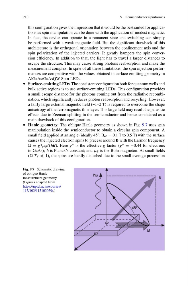
• Hanle geometry: The oblique Hanle geometry as shown in Fig. 9.7 uses spin
manipulation inside the semiconductor to obtain a circular spin component. A
small field applied at an angle (ideally 45°, B 45 = 0.1 T to 0.5 T) with the surface
causes the injected electron spins to precess around B with the Larmor frequency
= g*μ B / (èB). Here g* is the effective g factor (g* = −0.44 for electrons
in GaAs); è is Planck’s constant; and μ B is the Bohr magneton. At small fields
( T S 1), the spins are hardly disturbed due to the small average precession
Fig. 9.7 Schematic drawing
of oblique Hanle
measurement geometry
(Figures adapted from
https://nptel.ac.in/courses/
115/103/115103039/.)
9 Semiconductor Spintronics
this configuration gives the impression that it would be the best suited for applications as spin manipulation can be done with the application of modest magnetic.
In fact, the device can operate in a remanent state and switching can simply
be performed with a weak magnetic field. But the significant drawback of this
architecture is the orthogonal orientation between the confinement axis and the
spin polarization of the injected carriers. It greatly hampers the spin conversion efficiency. In addition to that, the light has to travel a larger distances to
escape the structure. This may cause strong photons reabsorption and make the
measurement complex. In spite of all these limitations, the spin injection performances are competitive with the values obtained in surface-emitting geometry in
AlGaAs/GaAsQW Spin-LEDs.
• Surface-emitting LEDs: The consistent configuration both for quantum wells and
bulk active regions is to use surface-emitting LEDs. This configuration provides
a small escape distance for the photons coming out from the radiative recombination, which significantly reduces photon reabsorption and recycling. However,
a fairly large external magnetic field (~1–2 T) is required to overcome the shape
anisotropy of the ferromagnetic thin layer. This large field may result the parasitic
effects due to Zeeman splitting in the semiconductor and hence considered as a
main drawback of this configuration.
• Hanle geometry: The oblique Hanle geometry as shown in Fig. 9.7 uses spin
manipulation inside the semiconductor to obtain a circular spin component. A
small field applied at an angle (ideally 45°, B 45 = 0.1 T to 0.5 T) with the surface
causes the injected electron spins to precess around B with the Larmor frequency
= g*μ B / (èB). Here g* is the effective g factor (g* = −0.44 for electrons
in GaAs); è is Planck’s constant; and μ B is the Bohr magneton. At small fields
( T S 1), the spins are hardly disturbed due to the small average precession
Fig. 9.7 Schematic drawing
of oblique Hanle
measurement geometry
(Figures adapted from
https://nptel.ac.in/courses/
115/103/115103039/.)