

3.3 Design for Test
77
Table 3.4 Scan chain information
Design
version
Nonscannable
flip-flops
Nonscannable
latches
Scannable
flip-flops
Flip-flops part
of a scan chain
Coverage
2
3519 (2.8 %) 1544 (1.2 %) 121 411
(96 %)
121 295
(95.9 %)
91 %
3
2646 (2.1 %) 72 (0.1 %)
123 026
(97.8 %)
122 980
(97.8 %)
92 %
value of the next state is captured in the chain. This state can then be shifted out and
compared against the expected one. By varying the state that is set up, most of the
in-between logic functionality can be verified. As the state space is very big, it is
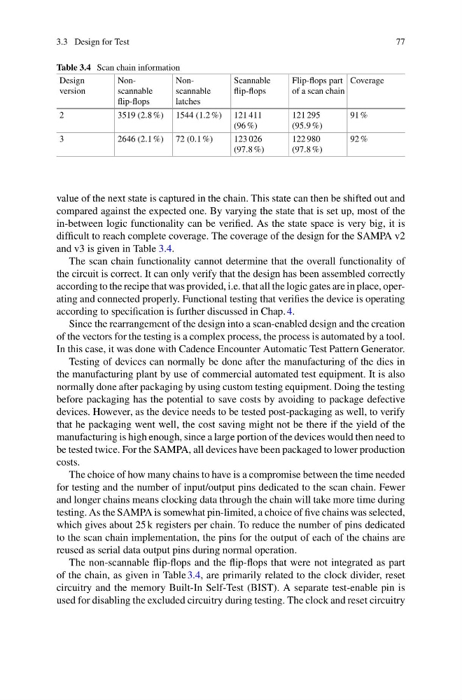
difficult to reach complete coverage. The coverage of the design for the SAMPA v2
and v3 is given in Table 3.4.
The scan chain functionality cannot determine that the overall functionality of
the circuit is correct. It can only verify that the design has been assembled correctly
according to the recipe that was provided, i.e. that all the logic gates are in place, operating and connected properly. Functional testing that verifies the device is operating
according to specification is further discussed in Chap. 4.
Since the rearrangement of the design into a scan-enabled design and the creation
of the vectors for the testing is a complex process, the process is automated by a tool.
In this case, it was done with Cadence Encounter Automatic Test Pattern Generator.
Testing of devices can normally be done after the manufacturing of the dies in
the manufacturing plant by use of commercial automated test equipment. It is also
normally done after packaging by using custom testing equipment. Doing the testing
before packaging has the potential to save costs by avoiding to package defective
devices. However, as the device needs to be tested post-packaging as well, to verify
that he packaging went well, the cost saving might not be there if the yield of the
manufacturing is high enough, since a large portion of the devices would then need to
be tested twice. For the SAMPA, all devices have been packaged to lower production
costs.
The choice of how many chains to have is a compromise between the time needed
for testing and the number of input/output pins dedicated to the scan chain. Fewer
and longer chains means clocking data through the chain will take more time during
testing. As the SAMPA is somewhat pin-limited, a choice of five chains was selected,
which gives about 25 k registers per chain. To reduce the number of pins dedicated
to the scan chain implementation, the pins for the output of each of the chains are
reused as serial data output pins during normal operation.
The non-scannable flip-flops and the flip-flops that were not integrated as part
of the chain, as given in Table 3.4, are primarily related to the clock divider, reset
circuitry and the memory Built-In Self-Test (BIST). A separate test-enable pin is
used for disabling the excluded circuitry during testing. The clock and reset circuitry
77
Table 3.4 Scan chain information
Design
version
Nonscannable
flip-flops
Nonscannable
latches
Scannable
flip-flops
Flip-flops part
of a scan chain
Coverage
2
3519 (2.8 %) 1544 (1.2 %) 121 411
(96 %)
121 295
(95.9 %)
91 %
3
2646 (2.1 %) 72 (0.1 %)
123 026
(97.8 %)
122 980
(97.8 %)
92 %
value of the next state is captured in the chain. This state can then be shifted out and
compared against the expected one. By varying the state that is set up, most of the
in-between logic functionality can be verified. As the state space is very big, it is
difficult to reach complete coverage. The coverage of the design for the SAMPA v2
and v3 is given in Table 3.4.
The scan chain functionality cannot determine that the overall functionality of
the circuit is correct. It can only verify that the design has been assembled correctly
according to the recipe that was provided, i.e. that all the logic gates are in place, operating and connected properly. Functional testing that verifies the device is operating
according to specification is further discussed in Chap. 4.
Since the rearrangement of the design into a scan-enabled design and the creation
of the vectors for the testing is a complex process, the process is automated by a tool.
In this case, it was done with Cadence Encounter Automatic Test Pattern Generator.
Testing of devices can normally be done after the manufacturing of the dies in
the manufacturing plant by use of commercial automated test equipment. It is also
normally done after packaging by using custom testing equipment. Doing the testing
before packaging has the potential to save costs by avoiding to package defective
devices. However, as the device needs to be tested post-packaging as well, to verify
that he packaging went well, the cost saving might not be there if the yield of the
manufacturing is high enough, since a large portion of the devices would then need to
be tested twice. For the SAMPA, all devices have been packaged to lower production
costs.
The choice of how many chains to have is a compromise between the time needed
for testing and the number of input/output pins dedicated to the scan chain. Fewer
and longer chains means clocking data through the chain will take more time during
testing. As the SAMPA is somewhat pin-limited, a choice of five chains was selected,
which gives about 25 k registers per chain. To reduce the number of pins dedicated
to the scan chain implementation, the pins for the output of each of the chains are
reused as serial data output pins during normal operation.
The non-scannable flip-flops and the flip-flops that were not integrated as part
of the chain, as given in Table 3.4, are primarily related to the clock divider, reset
circuitry and the memory Built-In Self-Test (BIST). A separate test-enable pin is
used for disabling the excluded circuitry during testing. The clock and reset circuitry