

3.2 Digital Implementation
53
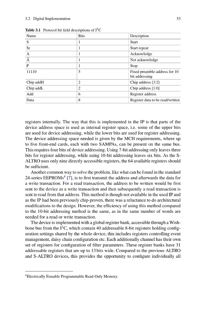
Table 3.1 Protocol bit field descriptions of I 2 C
Name
Bits
Description
S
1
Start
Sr
1
Start repeat
A
1
Acknowledge
A
1
Not acknowledge
P
1
Stop
11110
5
Fixed preamble address for 10
bit addressing
Chip addH
2
Chip address [3:2]
Chip addL
2
Chip address [1:0]
Add
6
Register address
Data
8
Register data to be read/written
registers internally. The way that this is implemented in the IP is that parts of the
device address space is used as internal register space, i.e. some of the upper bits
are used for device addressing, while the lower bits are used for register addressing.
The device addressing space needed is given by the MCH requirements, where up
to five front-end cards, each with two SAMPAs, can be present on the same bus.
This requires four bits of device addressing. Using 7-bit addressing only leaves three
bits for register addressing, while using 10-bit addressing leaves six bits. As the SALTRO uses only nine directly accessible registers, the 64 available registers should
be sufficient.
Another common way to solve the problem, like what can be found in the standard
24-series EEPROMs
4 [7], is to first transmit the address and afterwards the data for
a write transaction. For a read transaction, the address to be written would be first
sent to the device as a write transaction and then subsequently a read transaction is
sent to read from that address. This method is though not available in the used IP and
as the IP had been previously chip-proven, there was a reluctance to do architectural
modifications to the design. However, the efficiency of using this method compared
to the 10-bit addressing method is the same, as in the same number of words are
needed for a read or write transaction.
The device is implemented with a global register bank, accessible through a Wishbone bus from the I
2 C, which contain 40 addressable 8-bit registers holding configuration settings shared by the whole device, this includes registers controlling event
management, daisy chain configuration etc. Each additionally channel has their own
set of registers for configuration of filter parameters. These register banks have 31
addressable registers that are up to 13 bits wide. Compared to the previous ALTRO
and S-ALTRO devices, this provides the opportunity to configure individually all
4 Electrically Erasable Programmable Read-Only Memory.
53
Table 3.1 Protocol bit field descriptions of I 2 C
Name
Bits
Description
S
1
Start
Sr
1
Start repeat
A
1
Acknowledge
A
1
Not acknowledge
P
1
Stop
11110
5
Fixed preamble address for 10
bit addressing
Chip addH
2
Chip address [3:2]
Chip addL
2
Chip address [1:0]
Add
6
Register address
Data
8
Register data to be read/written
registers internally. The way that this is implemented in the IP is that parts of the
device address space is used as internal register space, i.e. some of the upper bits
are used for device addressing, while the lower bits are used for register addressing.
The device addressing space needed is given by the MCH requirements, where up
to five front-end cards, each with two SAMPAs, can be present on the same bus.
This requires four bits of device addressing. Using 7-bit addressing only leaves three
bits for register addressing, while using 10-bit addressing leaves six bits. As the SALTRO uses only nine directly accessible registers, the 64 available registers should
be sufficient.
Another common way to solve the problem, like what can be found in the standard
24-series EEPROMs
4 [7], is to first transmit the address and afterwards the data for
a write transaction. For a read transaction, the address to be written would be first
sent to the device as a write transaction and then subsequently a read transaction is
sent to read from that address. This method is though not available in the used IP and
as the IP had been previously chip-proven, there was a reluctance to do architectural
modifications to the design. However, the efficiency of using this method compared
to the 10-bit addressing method is the same, as in the same number of words are
needed for a read or write transaction.
The device is implemented with a global register bank, accessible through a Wishbone bus from the I
2 C, which contain 40 addressable 8-bit registers holding configuration settings shared by the whole device, this includes registers controlling event
management, daisy chain configuration etc. Each additionally channel has their own
set of registers for configuration of filter parameters. These register banks have 31
addressable registers that are up to 13 bits wide. Compared to the previous ALTRO
and S-ALTRO devices, this provides the opportunity to configure individually all
4 Electrically Erasable Programmable Read-Only Memory.