

52
3 SAMPA Chip Implementation
internally route one of the trigger inputs to the serial output. On the readout system
it is then possible to count the number of cycles it takes from a pulse is sent to it is
received again and by halving this, the length of the propagation delay can be found
to within one clock cycle.
3.2.2 Slow Control and Configuration
The slow control of the SAMPA is managed through I
2 C [6], using the 10-bit addressing scheme with automatic address increment on continued read/write operations.
The design is based on an Intellectual Property (IP) block created by CERN.
The I
2 C interface is designed to operate from 100 kHz to 5 MHz, which covers
the most common speeds listed in the standard; standard mode (100 kHz), fast mode
(400 kHz) and fast mode plus (1 MHz). Due to the need to operate at different speeds,
the internal state machine is relying on the clocking supplied by the I
2 C master to
advance its state. In case something goes wrong during the transmission, there is the
potential that the state machine will get stuck in an intermediary state. A watchdog
is implemented that will time out and return the state machine to idle if the time
between two falling edges of the I
2 C clock line is more than 512 bunch crossing
clock cycles apart (generally about 12.5 µs). This in sense sets the lower operating
speed of the I
2 C for the device. As the I
2 C state machine operates at the bunch
crossing clock frequency, nominally about 40 MHz, the design does not need to halt
the communication to complete internal read/write tasks, even at the highest transfer
speed, and so does not implement any clock stretching. The communication protocol
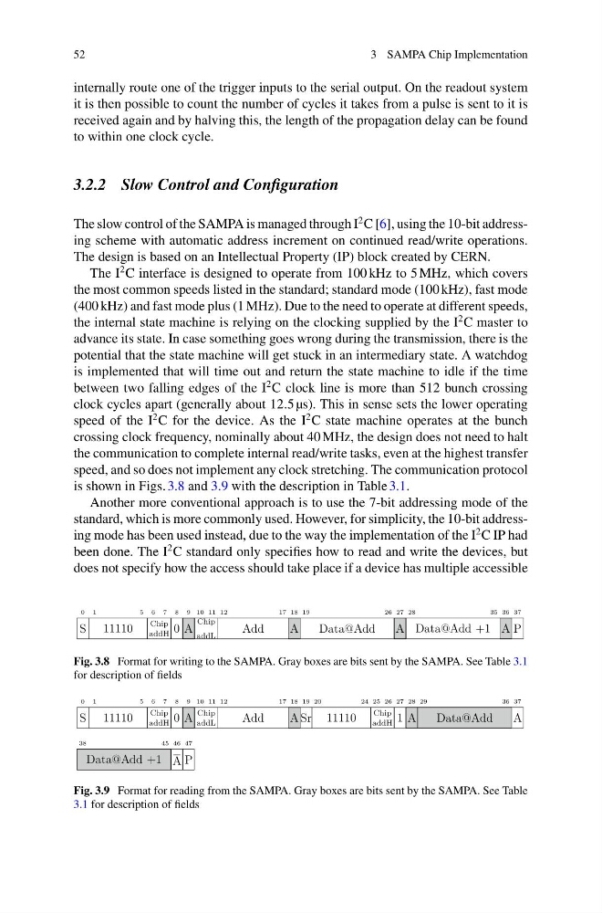
is shown in Figs. 3.8 and 3.9 with the description in Table 3.1.
Another more conventional approach is to use the 7-bit addressing mode of the
standard, which is more commonly used. However, for simplicity, the 10-bit addressing mode has been used instead, due to the way the implementation of the I
2 C IP had
been done. The I
2 C standard only specifies how to read and write the devices, but
does not specify how the access should take place if a device has multiple accessible
0 1
5 6 7 8 9 10 11 12
17 18 19
26 27 28
35 36 37
S 11110
Chip
addH 0 A
Chip
addL
Add
A
Data@Add
A Data@Add +1 A P
Fig. 3.8 Format for writing to the SAMPA. Gray boxes are bits sent by the SAMPA. See Table 3.1
for description of fields
0 1
5 6 7 8 9 10 11 12
17 18 19 20
24 25 26 27 28 29
36 37
S 11110
Chip
addH 0 A
Chip
addL
Add
A Sr 11110
Chip
addH 1 A
Data@Add
A
7
4
6
4
5
4
8
3
Data@Add +1 A P
Fig. 3.9 Format for reading from the SAMPA. Gray boxes are bits sent by the SAMPA. See Table
3.1 for description of fields
3 SAMPA Chip Implementation
internally route one of the trigger inputs to the serial output. On the readout system
it is then possible to count the number of cycles it takes from a pulse is sent to it is
received again and by halving this, the length of the propagation delay can be found
to within one clock cycle.
3.2.2 Slow Control and Configuration
The slow control of the SAMPA is managed through I
2 C [6], using the 10-bit addressing scheme with automatic address increment on continued read/write operations.
The design is based on an Intellectual Property (IP) block created by CERN.
The I
2 C interface is designed to operate from 100 kHz to 5 MHz, which covers
the most common speeds listed in the standard; standard mode (100 kHz), fast mode
(400 kHz) and fast mode plus (1 MHz). Due to the need to operate at different speeds,
the internal state machine is relying on the clocking supplied by the I
2 C master to
advance its state. In case something goes wrong during the transmission, there is the
potential that the state machine will get stuck in an intermediary state. A watchdog
is implemented that will time out and return the state machine to idle if the time
between two falling edges of the I
2 C clock line is more than 512 bunch crossing
clock cycles apart (generally about 12.5 µs). This in sense sets the lower operating
speed of the I
2 C for the device. As the I
2 C state machine operates at the bunch
crossing clock frequency, nominally about 40 MHz, the design does not need to halt
the communication to complete internal read/write tasks, even at the highest transfer
speed, and so does not implement any clock stretching. The communication protocol
is shown in Figs. 3.8 and 3.9 with the description in Table 3.1.
Another more conventional approach is to use the 7-bit addressing mode of the
standard, which is more commonly used. However, for simplicity, the 10-bit addressing mode has been used instead, due to the way the implementation of the I
2 C IP had
been done. The I
2 C standard only specifies how to read and write the devices, but
does not specify how the access should take place if a device has multiple accessible
0 1
5 6 7 8 9 10 11 12
17 18 19
26 27 28
35 36 37
S 11110
Chip
addH 0 A
Chip
addL
Add
A
Data@Add
A Data@Add +1 A P
Fig. 3.8 Format for writing to the SAMPA. Gray boxes are bits sent by the SAMPA. See Table 3.1
for description of fields
0 1
5 6 7 8 9 10 11 12
17 18 19 20
24 25 26 27 28 29
36 37
S 11110
Chip
addH 0 A
Chip
addL
Add
A Sr 11110
Chip
addH 1 A
Data@Add
A
7
4
6
4
5
4
8
3
Data@Add +1 A P
Fig. 3.9 Format for reading from the SAMPA. Gray boxes are bits sent by the SAMPA. See Table
3.1 for description of fields