

50
3 SAMPA Chip Implementation
D
Q
D
Q
Serial clk un-gated
'1'
Hard reset pin (n)
BX clk
ADC clk un-gated
Power-on reset pin (n)
D
Q
D
Q
'1'
D
Q
D
Q
'1'
D
Q
D
Q
'1'
D
Q
D
Q
'1'
Serial clk
Serial clk div 2
Soft reset
D
Q
D
Q
D
Q
D
Q
D
Q
D
Q
async
async
async
async
async
async
async
async
async
async
Hard reset (n)
serial clk
Hard reset
ADC clk
(For registers)
Hard & soft reset (n)
ADC clk
Hard & soft reset (n)
BX clk
Hard & soft reset (n)
serial clk div 2
Hard & soft reset (n)
serial clk
320/160/80 MHz
160/80/40 MHz
40 MHz
5-20 MHz
320/160/80 MHz
D
Q
SDA output enable (n)
D
Q
Hold soft reset until I2C ACK done
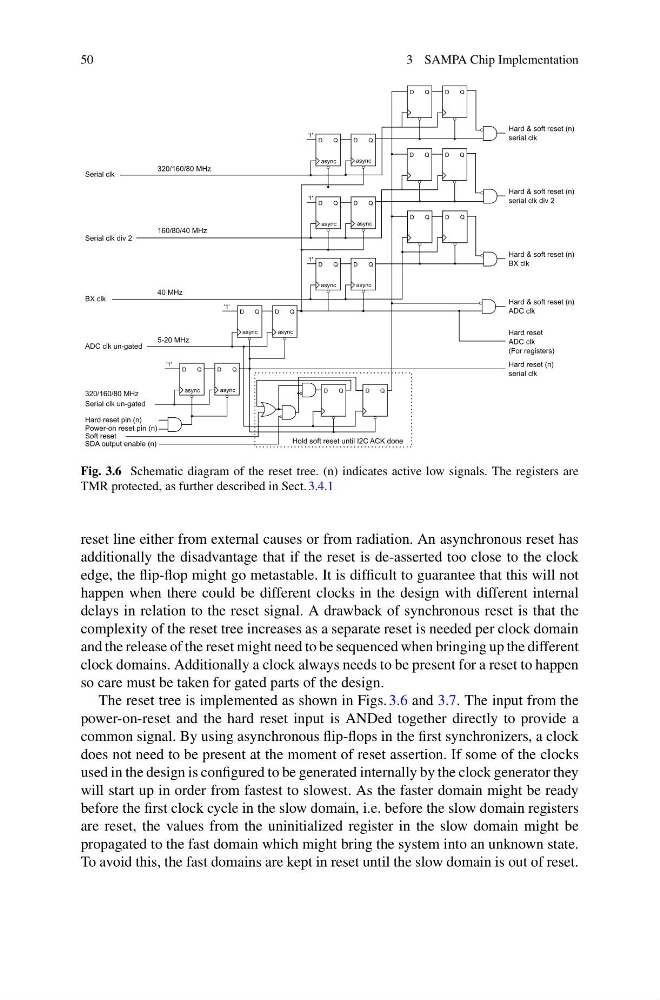
Fig. 3.6 Schematic diagram of the reset tree. (n) indicates active low signals. The registers are
TMR protected, as further described in Sect. 3.4.1
reset line either from external causes or from radiation. An asynchronous reset has
additionally the disadvantage that if the reset is de-asserted too close to the clock
edge, the flip-flop might go metastable. It is difficult to guarantee that this will not
happen when there could be different clocks in the design with different internal
delays in relation to the reset signal. A drawback of synchronous reset is that the
complexity of the reset tree increases as a separate reset is needed per clock domain
and the release of the reset might need to be sequenced when bringing up the different
clock domains. Additionally a clock always needs to be present for a reset to happen
so care must be taken for gated parts of the design.
The reset tree is implemented as shown in Figs. 3.6 and 3.7. The input from the
power-on-reset and the hard reset input is ANDed together directly to provide a
common signal. By using asynchronous flip-flops in the first synchronizers, a clock
does not need to be present at the moment of reset assertion. If some of the clocks
used in the design is configured to be generated internally by the clock generator they
will start up in order from fastest to slowest. As the faster domain might be ready
before the first clock cycle in the slow domain, i.e. before the slow domain registers
are reset, the values from the uninitialized register in the slow domain might be
propagated to the fast domain which might bring the system into an unknown state.
To avoid this, the fast domains are kept in reset until the slow domain is out of reset.
3 SAMPA Chip Implementation
D
Q
D
Q
Serial clk un-gated
'1'
Hard reset pin (n)
BX clk
ADC clk un-gated
Power-on reset pin (n)
D
Q
D
Q
'1'
D
Q
D
Q
'1'
D
Q
D
Q
'1'
D
Q
D
Q
'1'
Serial clk
Serial clk div 2
Soft reset
D
Q
D
Q
D
Q
D
Q
D
Q
D
Q
async
async
async
async
async
async
async
async
async
async
Hard reset (n)
serial clk
Hard reset
ADC clk
(For registers)
Hard & soft reset (n)
ADC clk
Hard & soft reset (n)
BX clk
Hard & soft reset (n)
serial clk div 2
Hard & soft reset (n)
serial clk
320/160/80 MHz
160/80/40 MHz
40 MHz
5-20 MHz
320/160/80 MHz
D
Q
SDA output enable (n)
D
Q
Hold soft reset until I2C ACK done
Fig. 3.6 Schematic diagram of the reset tree. (n) indicates active low signals. The registers are
TMR protected, as further described in Sect. 3.4.1
reset line either from external causes or from radiation. An asynchronous reset has
additionally the disadvantage that if the reset is de-asserted too close to the clock
edge, the flip-flop might go metastable. It is difficult to guarantee that this will not
happen when there could be different clocks in the design with different internal
delays in relation to the reset signal. A drawback of synchronous reset is that the
complexity of the reset tree increases as a separate reset is needed per clock domain
and the release of the reset might need to be sequenced when bringing up the different
clock domains. Additionally a clock always needs to be present for a reset to happen
so care must be taken for gated parts of the design.
The reset tree is implemented as shown in Figs. 3.6 and 3.7. The input from the
power-on-reset and the hard reset input is ANDed together directly to provide a
common signal. By using asynchronous flip-flops in the first synchronizers, a clock
does not need to be present at the moment of reset assertion. If some of the clocks
used in the design is configured to be generated internally by the clock generator they
will start up in order from fastest to slowest. As the faster domain might be ready
before the first clock cycle in the slow domain, i.e. before the slow domain registers
are reset, the values from the uninitialized register in the slow domain might be
propagated to the fast domain which might bring the system into an unknown state.
To avoid this, the fast domains are kept in reset until the slow domain is out of reset.