

3.1 Architectural Overview
43
C f
R f
R pz
C dif
R dif
Charge Sensitive Amp
C 2
C 3
R T
R T
C 2
C 3
R T
R T
R T
R T
C 3
C 2
Semi-Gaussian pulse Shaper
V out+
V outR G
R G
-A 1
-A 2
-A 2
V CM
750mV
450mV
1.1V
0.1V
NIS
600mV
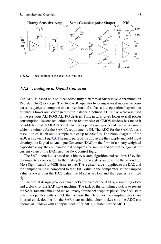
Fig. 3.2 Block diagram of the analogue front-end
3.1.2 Analogue to Digital Converter
The ADC is based on a split capacitor fully differential Successive Approximation
Register (SAR) topology. The SAR ADC operates by doing several successive comparisons cycles to complete one conversion and so has a low operational speed, but
requires a lower area compared to for instance pipelined ADCs like what was used
in the previous ALTRO/S-ALTRO devices. This, in turn, gives lower overall power
consumption. Recent reductions in the feature size of CMOS devices has made it
possible to create SAR ADCs that can reach operational speeds and have an accuracy
which is suitable for the SAMPA requirements [3]. The ADC for the SAMPA has a
resolution of 10-bit and a sample rate of up to 20 MS/s. The block diagram of the
ADC is shown in Fig. 3.3. The main parts of the circuit are the sample and hold input
circuitry, the Digital to Analogue Converter (DAC) in the form of a binary weighted
capacitive array, the comparator that compares the sample and hold value against the
current value of the DAC, and the SAR control logic.
The SAR operation is based on a binary search algorithm and requires 12 cycles
to complete a conversion. In the first cycle, the registers are reset, in the second the
Most Significant Bit (MSB) is set to one. The register value is applied to the DAC and
the sampled value is compared to the DAC value in the comparator. If the sampled
value is lower than the DAQ value, the MSB is set low and the register is shifted
right.
The digital design provides two clocks for each of the ADCs, a sampling clock
and a clock for the SAR state machine. The task of the sampling clock is to restart
the SAR state machines and make it ready for the next capture phase. The SAR state
machine operates with a clock that is more than 16 times the sampling clock. An
internal clock doubler for the SAR state machine clock makes sure the ADC can
operate at 10 MS/s with an input clock of 80 MHz, suitable for the MCH.
43
C f
R f
R pz
C dif
R dif
Charge Sensitive Amp
C 2
C 3
R T
R T
C 2
C 3
R T
R T
R T
R T
C 3
C 2
Semi-Gaussian pulse Shaper
V out+
V outR G
R G
-A 1
-A 2
-A 2
V CM
750mV
450mV
1.1V
0.1V
NIS
600mV
Fig. 3.2 Block diagram of the analogue front-end
3.1.2 Analogue to Digital Converter
The ADC is based on a split capacitor fully differential Successive Approximation
Register (SAR) topology. The SAR ADC operates by doing several successive comparisons cycles to complete one conversion and so has a low operational speed, but
requires a lower area compared to for instance pipelined ADCs like what was used
in the previous ALTRO/S-ALTRO devices. This, in turn, gives lower overall power
consumption. Recent reductions in the feature size of CMOS devices has made it
possible to create SAR ADCs that can reach operational speeds and have an accuracy
which is suitable for the SAMPA requirements [3]. The ADC for the SAMPA has a
resolution of 10-bit and a sample rate of up to 20 MS/s. The block diagram of the
ADC is shown in Fig. 3.3. The main parts of the circuit are the sample and hold input
circuitry, the Digital to Analogue Converter (DAC) in the form of a binary weighted
capacitive array, the comparator that compares the sample and hold value against the
current value of the DAC, and the SAR control logic.
The SAR operation is based on a binary search algorithm and requires 12 cycles
to complete a conversion. In the first cycle, the registers are reset, in the second the
Most Significant Bit (MSB) is set to one. The register value is applied to the DAC and
the sampled value is compared to the DAC value in the comparator. If the sampled
value is lower than the DAQ value, the MSB is set low and the register is shifted
right.
The digital design provides two clocks for each of the ADCs, a sampling clock
and a clock for the SAR state machine. The task of the sampling clock is to restart
the SAR state machines and make it ready for the next capture phase. The SAR state
machine operates with a clock that is more than 16 times the sampling clock. An
internal clock doubler for the SAR state machine clock makes sure the ADC can
operate at 10 MS/s with an input clock of 80 MHz, suitable for the MCH.