

Appendix B: Registers
147
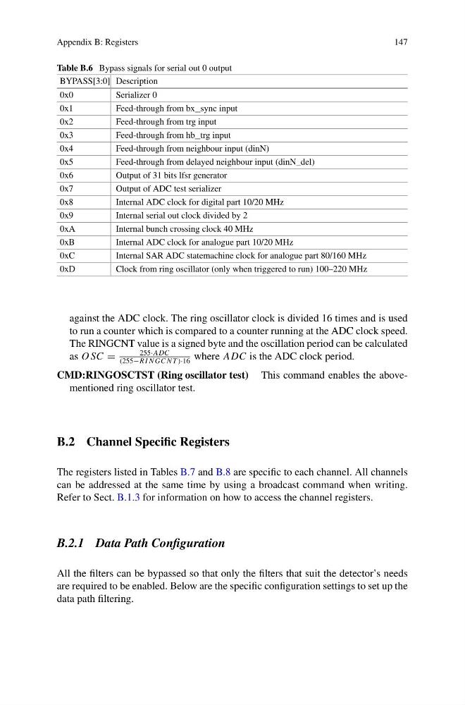
Table B.6 Bypass signals for serial out 0 output
BYPASS[3:0] Description
0x0
Serializer 0
0x1
Feed-through from bx_sync input
0x2
Feed-through from trg input
0x3
Feed-through from hb_trg input
0x4
Feed-through from neighbour input (dinN)
0x5
Feed-through from delayed neighbour input (dinN_del)
0x6
Output of 31 bits lfsr generator
0x7
Output of ADC test serializer
0x8
Internal ADC clock for digital part 10/20 MHz
0x9
Internal serial out clock divided by 2
0xA
Internal bunch crossing clock 40 MHz
0xB
Internal ADC clock for analogue part 10/20 MHz
0xC
Internal SAR ADC statemachine clock for analogue part 80/160 MHz
0xD
Clock from ring oscillator (only when triggered to run) 100–220 MHz
against the ADC clock. The ring oscillator clock is divided 16 times and is used
to run a counter which is compared to a counter running at the ADC clock speed.
The RINGCNT value is a signed byte and the oscillation period can be calculated
as O SC =
255·ADC
(255−R I N GC N T )·16
where ADC is the ADC clock period.
CMD:RINGOSCTST (Ring oscillator test) This command enables the abovementioned ring oscillator test.
B.2 Channel Specific Registers
The registers listed in Tables B.7 and B.8 are specific to each channel. All channels
can be addressed at the same time by using a broadcast command when writing.
Refer to Sect. B.1.3 for information on how to access the channel registers.
B.2.1 Data Path Configuration
All the filters can be bypassed so that only the filters that suit the detector’s needs
are required to be enabled. Below are the specific configuration settings to set up the
data path filtering.
147
Table B.6 Bypass signals for serial out 0 output
BYPASS[3:0] Description
0x0
Serializer 0
0x1
Feed-through from bx_sync input
0x2
Feed-through from trg input
0x3
Feed-through from hb_trg input
0x4
Feed-through from neighbour input (dinN)
0x5
Feed-through from delayed neighbour input (dinN_del)
0x6
Output of 31 bits lfsr generator
0x7
Output of ADC test serializer
0x8
Internal ADC clock for digital part 10/20 MHz
0x9
Internal serial out clock divided by 2
0xA
Internal bunch crossing clock 40 MHz
0xB
Internal ADC clock for analogue part 10/20 MHz
0xC
Internal SAR ADC statemachine clock for analogue part 80/160 MHz
0xD
Clock from ring oscillator (only when triggered to run) 100–220 MHz
against the ADC clock. The ring oscillator clock is divided 16 times and is used
to run a counter which is compared to a counter running at the ADC clock speed.
The RINGCNT value is a signed byte and the oscillation period can be calculated
as O SC =
255·ADC
(255−R I N GC N T )·16
where ADC is the ADC clock period.
CMD:RINGOSCTST (Ring oscillator test) This command enables the abovementioned ring oscillator test.
B.2 Channel Specific Registers
The registers listed in Tables B.7 and B.8 are specific to each channel. All channels
can be addressed at the same time by using a broadcast command when writing.
Refer to Sect. B.1.3 for information on how to access the channel registers.
B.2.1 Data Path Configuration
All the filters can be bypassed so that only the filters that suit the detector’s needs
are required to be enabled. Below are the specific configuration settings to set up the
data path filtering.