

138
Appendix B: Registers
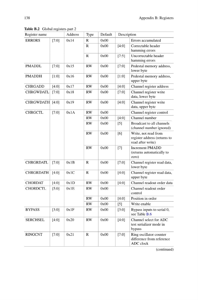
Table B.2 Global registers part 2
Register name
Address
Type
Default
Description
ERRORS
[7:0]
0x14
R
0x00
Errors accumulated
R
0x00
[4:0]
Correctable header
hamming errors
R
0x00
[7:5]
Uncorrectable header
hamming errors
PMADDL
[7:0]
0x15
RW
0x00
[7:0]
Pedestal memory address,
lower byte
PMADDH
[1:0]
0x16
RW
0x00
[1:0]
Pedestal memory address,
upper byte
CHRGADD
[4:0]
0x17
RW
0x00
[4:0]
Channel register address
CHRGWDATL [7:0]
0x18
RW
0x00
[7:0]
Channel register write
data, lower byte
CHRGWDATH [4:0]
0x19
RW
0x00
[4:0]
Channel register write
data, upper byte
CHRGCTL
[7:0]
0x1A
RW
0x00
Channel register control
RW
0x00
[4:0]
Channel number
RW
0x00
[5]
Broadcast to all channels
(channel number ignored)
RW
0x00
[6]
Write, not read from
register address (returns to
read after write)
RW
0x00
[7]
Increment PMADD
(returns automatically to
zero)
CHRGRDATL [7:0]
0x1B
R
0x00
[7:0]
Channel register read data,
lower byte
CHRGRDATH [4:0]
0x1C
R
0x00
[4:0]
Channel register read data,
upper byte
CHORDAT
[4:0]
0x1D
RW
0x00
[4:0]
Channel readout order data
CHORDCTL
[5:0]
0x1E
RW
0x00
Channel readout order
control
RW
0x00
[4:0]
Position in order
RW
0x00
[5]
Write enable
BYPASS
[3:0]
0x1F
RW
0x00
[3:0]
Bypass inputs to serial 0,
see Table B.6
SERCHSEL
[4:0]
0x20
RW
0x00
[4:0]
Channel select for ADC
test serializer mode in
bypass
RINGCNT
[7:0]
0x21
R
0x00
[7:0]
Ring oscillator counter
difference from reference
ADC clock
(continued)
Appendix B: Registers
Table B.2 Global registers part 2
Register name
Address
Type
Default
Description
ERRORS
[7:0]
0x14
R
0x00
Errors accumulated
R
0x00
[4:0]
Correctable header
hamming errors
R
0x00
[7:5]
Uncorrectable header
hamming errors
PMADDL
[7:0]
0x15
RW
0x00
[7:0]
Pedestal memory address,
lower byte
PMADDH
[1:0]
0x16
RW
0x00
[1:0]
Pedestal memory address,
upper byte
CHRGADD
[4:0]
0x17
RW
0x00
[4:0]
Channel register address
CHRGWDATL [7:0]
0x18
RW
0x00
[7:0]
Channel register write
data, lower byte
CHRGWDATH [4:0]
0x19
RW
0x00
[4:0]
Channel register write
data, upper byte
CHRGCTL
[7:0]
0x1A
RW
0x00
Channel register control
RW
0x00
[4:0]
Channel number
RW
0x00
[5]
Broadcast to all channels
(channel number ignored)
RW
0x00
[6]
Write, not read from
register address (returns to
read after write)
RW
0x00
[7]
Increment PMADD
(returns automatically to
zero)
CHRGRDATL [7:0]
0x1B
R
0x00
[7:0]
Channel register read data,
lower byte
CHRGRDATH [4:0]
0x1C
R
0x00
[4:0]
Channel register read data,
upper byte
CHORDAT
[4:0]
0x1D
RW
0x00
[4:0]
Channel readout order data
CHORDCTL
[5:0]
0x1E
RW
0x00
Channel readout order
control
RW
0x00
[4:0]
Position in order
RW
0x00
[5]
Write enable
BYPASS
[3:0]
0x1F
RW
0x00
[3:0]
Bypass inputs to serial 0,
see Table B.6
SERCHSEL
[4:0]
0x20
RW
0x00
[4:0]
Channel select for ADC
test serializer mode in
bypass
RINGCNT
[7:0]
0x21
R
0x00
[7:0]
Ring oscillator counter
difference from reference
ADC clock
(continued)