

116
4 Verification and Testing
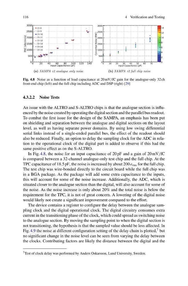
Fig. 4.8 Noise as a function of load capacitance at 20 mV/fC gain for the analogue-only 32 ch
front-end chip (left) and the full chip including ADC and DSP (right) [29]
4.3.2.2 Noise Tests
An issue with the ALTRO and S-ALTRO chips is that the analogue section is influenced by the noise created by operating the digital section and the parallel bus readout.
To combat the first issue for the design of the SAMPA, an emphasis has been put
on shielding and separation between the analogue and digital sections on the layout
level, as well as having separate power domains. By using low swing differential
serial links instead of a single-ended parallel bus, the effect of the readout should
also be reduced. Finally, an option to delay the sampling clock for the ADC in relation to the operational clock of the digital part is added to observe if this had the
same positive effect as on the S-ALTRO.
In Fig. 4.8, the noise for an input capacitance of 20 pF and a gain of 20 mV/fC
is compared between a 32-channel analogue-only test chip and the full chip. At the
TPC capacitance of 18.5 pF, the noise is increased by about 200 e rms for the full chip.
The test chip was wire-bonded directly to the circuit board while the full chip was
in a BGA package. As the package will add some extra capacitance to the inputs,
this will account for some of the noise increase. Additionally, the ADC, which is
situated closer to the analogue section than the digital, will also account for some of
the noise. As the noise increase is only about 20% and the total noise is below the
requirement for the TPC, it is not of great concern. A lowering of the digital noise
would likely not create a significant improvement compared to the effort.
The device contains a register to configure the delay between the analogue sampling clock and the digital operational clock. The digital circuitry consumes extra
current in the transitioning phase of the clock, which could spread as switching noise
to the analogue section. By moving the sampling point to when the digital section is
not transitioning, the hypothesis is that the sampled value should be less affected. In
Fig. 4.9 the noise at different configuration setting of the delay chain is plotted,
7 but
no significant change in the noise level can be seen from varying the delay between
the clocks. Contributing factors are likely the distance between the digital and the
7 Test of clock delay was performed by Anders Oskarsson, Lund University, Sweden.
4 Verification and Testing
Fig. 4.8 Noise as a function of load capacitance at 20 mV/fC gain for the analogue-only 32 ch
front-end chip (left) and the full chip including ADC and DSP (right) [29]
4.3.2.2 Noise Tests
An issue with the ALTRO and S-ALTRO chips is that the analogue section is influenced by the noise created by operating the digital section and the parallel bus readout.
To combat the first issue for the design of the SAMPA, an emphasis has been put
on shielding and separation between the analogue and digital sections on the layout
level, as well as having separate power domains. By using low swing differential
serial links instead of a single-ended parallel bus, the effect of the readout should
also be reduced. Finally, an option to delay the sampling clock for the ADC in relation to the operational clock of the digital part is added to observe if this had the
same positive effect as on the S-ALTRO.
In Fig. 4.8, the noise for an input capacitance of 20 pF and a gain of 20 mV/fC
is compared between a 32-channel analogue-only test chip and the full chip. At the
TPC capacitance of 18.5 pF, the noise is increased by about 200 e rms for the full chip.
The test chip was wire-bonded directly to the circuit board while the full chip was
in a BGA package. As the package will add some extra capacitance to the inputs,
this will account for some of the noise increase. Additionally, the ADC, which is
situated closer to the analogue section than the digital, will also account for some of
the noise. As the noise increase is only about 20% and the total noise is below the
requirement for the TPC, it is not of great concern. A lowering of the digital noise
would likely not create a significant improvement compared to the effort.
The device contains a register to configure the delay between the analogue sampling clock and the digital operational clock. The digital circuitry consumes extra
current in the transitioning phase of the clock, which could spread as switching noise
to the analogue section. By moving the sampling point to when the digital section is
not transitioning, the hypothesis is that the sampled value should be less affected. In
Fig. 4.9 the noise at different configuration setting of the delay chain is plotted,
7 but
no significant change in the noise level can be seen from varying the delay between
the clocks. Contributing factors are likely the distance between the digital and the
7 Test of clock delay was performed by Anders Oskarsson, Lund University, Sweden.