

4.3 Validation and Testing
117
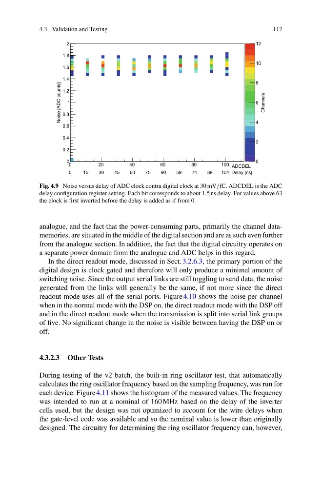
Fig. 4.9 Noise versus delay of ADC clock contra digital clock at 30 mV/fC. ADCDEL is the ADC
delay configuration register setting. Each bit corresponds to about 1.5 ns delay. For values above 63
the clock is first inverted before the delay is added as if from 0
analogue, and the fact that the power-consuming parts, primarily the channel datamemories, are situated in the middle of the digital section and are as such even further
from the analogue section. In addition, the fact that the digital circuitry operates on
a separate power domain from the analogue and ADC helps in this regard.
In the direct readout mode, discussed in Sect. 3.2.6.3, the primary portion of the
digital design is clock gated and therefore will only produce a minimal amount of
switching noise. Since the output serial links are still toggling to send data, the noise
generated from the links will generally be the same, if not more since the direct
readout mode uses all of the serial ports. Figure 4.10 shows the noise per channel
when in the normal mode with the DSP on, the direct readout mode with the DSP off
and in the direct readout mode when the transmission is split into serial link groups
of five. No significant change in the noise is visible between having the DSP on or
off.
4.3.2.3 Other Tests
During testing of the v2 batch, the built-in ring oscillator test, that automatically
calculates the ring oscillator frequency based on the sampling frequency, was run for
each device. Figure 4.11 shows the histogram of the measured values. The frequency
was intended to run at a nominal of 160 MHz based on the delay of the inverter
cells used, but the design was not optimized to account for the wire delays when
the gate-level code was available and so the nominal value is lower than originally
designed. The circuitry for determining the ring oscillator frequency can, however,
117
Fig. 4.9 Noise versus delay of ADC clock contra digital clock at 30 mV/fC. ADCDEL is the ADC
delay configuration register setting. Each bit corresponds to about 1.5 ns delay. For values above 63
the clock is first inverted before the delay is added as if from 0
analogue, and the fact that the power-consuming parts, primarily the channel datamemories, are situated in the middle of the digital section and are as such even further
from the analogue section. In addition, the fact that the digital circuitry operates on
a separate power domain from the analogue and ADC helps in this regard.
In the direct readout mode, discussed in Sect. 3.2.6.3, the primary portion of the
digital design is clock gated and therefore will only produce a minimal amount of
switching noise. Since the output serial links are still toggling to send data, the noise
generated from the links will generally be the same, if not more since the direct
readout mode uses all of the serial ports. Figure 4.10 shows the noise per channel
when in the normal mode with the DSP on, the direct readout mode with the DSP off
and in the direct readout mode when the transmission is split into serial link groups
of five. No significant change in the noise is visible between having the DSP on or
off.
4.3.2.3 Other Tests
During testing of the v2 batch, the built-in ring oscillator test, that automatically
calculates the ring oscillator frequency based on the sampling frequency, was run for
each device. Figure 4.11 shows the histogram of the measured values. The frequency
was intended to run at a nominal of 160 MHz based on the delay of the inverter
cells used, but the design was not optimized to account for the wire delays when
the gate-level code was available and so the nominal value is lower than originally
designed. The circuitry for determining the ring oscillator frequency can, however,