

3.5 Design for Low Power
89
when not used, disabling the clock to certain sections when not in use or by lowering
or turning off the supply voltage to certain sections.
The majority of the design operates at the lowest necessary speed, which is the
same as the ADC sampling speed. Only the circuitry between the ring buffers and the
serializers, which is a small part of the design, runs at a higher speed, and then only at
half the serialization speed. The parts that run at higher speed are also concentrated
furthest away from the analogue section to reduce the noise coupling. As the digital
part that runs at the ADC sampling speed will still create noise when the logic is
switching, there is a possibility that this could influence the sampling of the analogue
signal in the ADC. Therefore, a programmable delay chain has been implemented
for the sampling clock that goes to the ADCs so that the sampling can happen during
a quiet period. The delay chain used delay cells to implement the delay with a
granularity of 1.5 ns per bit for a maximum of 94.5 ns. The delay in a delay cell is
subject to process variations, temperature, and voltage variations, so if an accurate
delay is needed for keeping several devices in sync, it is also possible to only invert
the clock.
To avoid unnecessary toggling of data paths, the paths that are not in use are kept
at static values e.g. the inputs to filters that have been disabled and the address and
data ports for memories that are not currently activated.
Clock gating is used to disable the clock to circuitry that is not needed. For instance,
when the daisy chain mode is disabled, the clocks for the module that receives data
from the daisy chain are turned off. The I
2 C module enables its clock only between
a start bit and a stop bit, so it is effectively disabled when it is not receiving a word.
A watchdog makes sure the module returns to idle if a start is received, but the
transmission halts before a stop is received.
If a specific channel is determined to be defective or the device is used for an
application where not all of the channels are in use, it is possible to clock gate
the specific channel through a configuration register. This clock gating disables the
clocks to the ADC and prevents the digital processing chain of the channel to run,
though it does not clock gate the digital channel to avoid having 32 separate clock
trees. As the digital channels consume most of the area of the device, having separate
clock trees would likely negatively affect the routing of the device.
In the direct readout mode, only a very small part of the design is needed, primarily
the direct serialization module, the slow control, and the main configuration register.
Therefore, the clocks for the rest of the design are gated to save power. Enabling
of the clock gating is done through an external pin, which also enables the direct
readout mode.
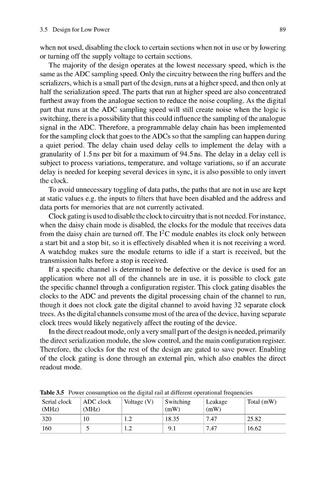
Table 3.5 Power consumption on the digital rail at different operational frequencies
Serial clock
(MHz)
ADC clock
(MHz)
Voltage (V)
Switching
(mW)
Leakage
(mW)
Total (mW)
320
10
1.2
18.35
7.47
25.82
160
5
1.2
9.1
7.47
16.62
89
when not used, disabling the clock to certain sections when not in use or by lowering
or turning off the supply voltage to certain sections.
The majority of the design operates at the lowest necessary speed, which is the
same as the ADC sampling speed. Only the circuitry between the ring buffers and the
serializers, which is a small part of the design, runs at a higher speed, and then only at
half the serialization speed. The parts that run at higher speed are also concentrated
furthest away from the analogue section to reduce the noise coupling. As the digital
part that runs at the ADC sampling speed will still create noise when the logic is
switching, there is a possibility that this could influence the sampling of the analogue
signal in the ADC. Therefore, a programmable delay chain has been implemented
for the sampling clock that goes to the ADCs so that the sampling can happen during
a quiet period. The delay chain used delay cells to implement the delay with a
granularity of 1.5 ns per bit for a maximum of 94.5 ns. The delay in a delay cell is
subject to process variations, temperature, and voltage variations, so if an accurate
delay is needed for keeping several devices in sync, it is also possible to only invert
the clock.
To avoid unnecessary toggling of data paths, the paths that are not in use are kept
at static values e.g. the inputs to filters that have been disabled and the address and
data ports for memories that are not currently activated.
Clock gating is used to disable the clock to circuitry that is not needed. For instance,
when the daisy chain mode is disabled, the clocks for the module that receives data
from the daisy chain are turned off. The I
2 C module enables its clock only between
a start bit and a stop bit, so it is effectively disabled when it is not receiving a word.
A watchdog makes sure the module returns to idle if a start is received, but the
transmission halts before a stop is received.
If a specific channel is determined to be defective or the device is used for an
application where not all of the channels are in use, it is possible to clock gate
the specific channel through a configuration register. This clock gating disables the
clocks to the ADC and prevents the digital processing chain of the channel to run,
though it does not clock gate the digital channel to avoid having 32 separate clock
trees. As the digital channels consume most of the area of the device, having separate
clock trees would likely negatively affect the routing of the device.
In the direct readout mode, only a very small part of the design is needed, primarily
the direct serialization module, the slow control, and the main configuration register.
Therefore, the clocks for the rest of the design are gated to save power. Enabling
of the clock gating is done through an external pin, which also enables the direct
readout mode.
Table 3.5 Power consumption on the digital rail at different operational frequencies
Serial clock
(MHz)
ADC clock
(MHz)
Voltage (V)
Switching
(mW)
Leakage
(mW)
Total (mW)
320
10
1.2
18.35
7.47
25.82
160
5
1.2
9.1
7.47
16.62