

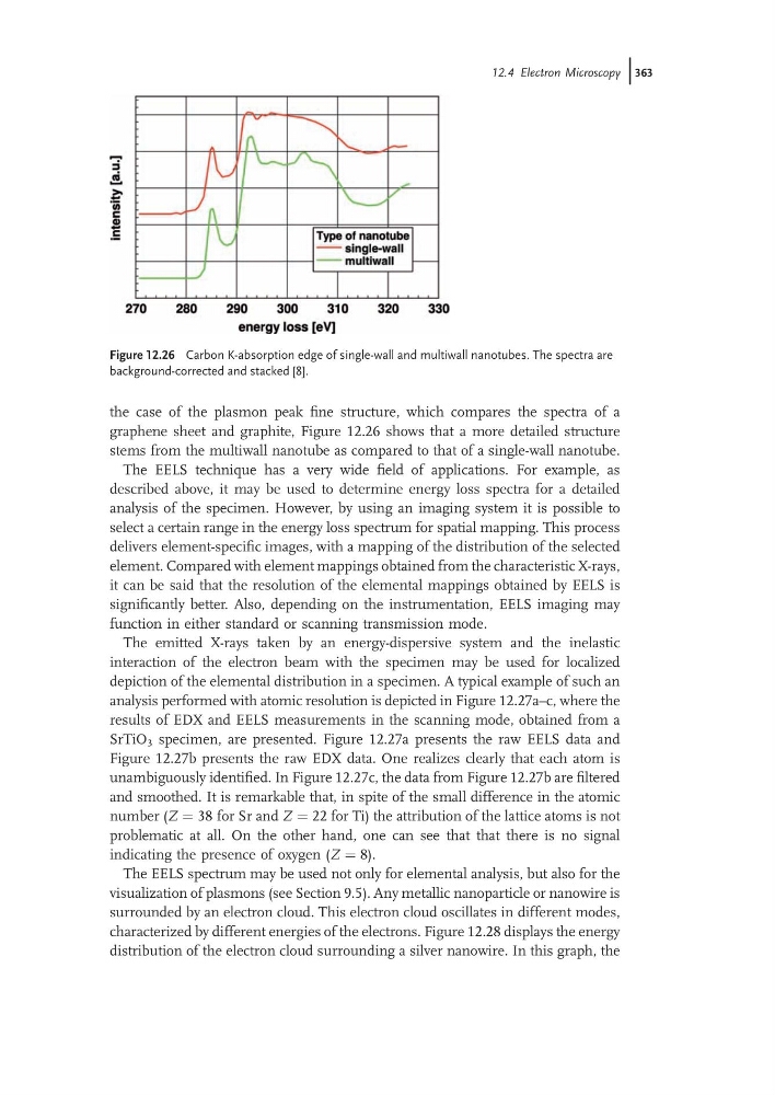
the case of the plasmon peak fine structure, which compares the spectra of a
graphene sheet and graphite, Figure 12.26 shows that a more detailed structure
stems from the multiwall nanotube as compared to that of a single-wall nanotube.
The EELS technique has a very wide field of applications. For example, as
described above, it may be used to determine energy loss spectra for a detailed
analysis of the specimen. However, by using an imaging system it is possible to
select a certain range in the energy loss spectrum for spatial mapping. This process
delivers element-specific images, with a mapping of the distribution of the selected
element. Compared with element mappings obtained from the characteristic X-rays,
it can be said that the resolution of the elemental mappings obtained by EELS is
significantly better. Also, depending on the instrumentation, EELS imaging may
function in either standard or scanning transmission mode.
The emitted X-rays taken by an energy-dispersive system and the inelastic
interaction of the electron beam with the specimen may be used for localized
depiction of the elemental distribution in a specimen. A typical example of such an
analysis performed with atomic resolution is depicted in Figure 12.27a–c, where the
results of EDX and EELS measurements in the scanning mode, obtained from a
SrTiO 3 specimen, are presented. Figure 12.27a presents the raw EELS data and
Figure 12.27b presents the raw EDX data. One realizes clearly that each atom is
unambiguously identified. In Figure 12.27c, the data from Figure 12.27b are filtered
and smoothed. It is remarkable that, in spite of the small difference in the atomic
number (Z ¼ 38 for Sr and Z ¼ 22 for Ti) the attribution of the lattice atoms is not
problematic at all. On the other hand, one can see that that there is no signal
indicating the presence of oxygen (Z ¼ 8).
The EELS spectrum may be used not only for elemental analysis, but also for the
visualization of plasmons (see Section 9.5). Any metallic nanoparticle or nanowire is
surrounded by an electron cloud. This electron cloud oscillates in different modes,
characterized by different energies of the electrons. Figure 12.28 displays the energy
distribution of the electron cloud surrounding a silver nanowire. In this graph, the
Figure 12.26 Carbon K-absorption edge of single-wall and multiwall nanotubes. The spectra are
background-corrected and stacked [8].
12.4 Electron Microscopy j363
graphene sheet and graphite, Figure 12.26 shows that a more detailed structure
stems from the multiwall nanotube as compared to that of a single-wall nanotube.
The EELS technique has a very wide field of applications. For example, as
described above, it may be used to determine energy loss spectra for a detailed
analysis of the specimen. However, by using an imaging system it is possible to
select a certain range in the energy loss spectrum for spatial mapping. This process
delivers element-specific images, with a mapping of the distribution of the selected
element. Compared with element mappings obtained from the characteristic X-rays,
it can be said that the resolution of the elemental mappings obtained by EELS is
significantly better. Also, depending on the instrumentation, EELS imaging may
function in either standard or scanning transmission mode.
The emitted X-rays taken by an energy-dispersive system and the inelastic
interaction of the electron beam with the specimen may be used for localized
depiction of the elemental distribution in a specimen. A typical example of such an
analysis performed with atomic resolution is depicted in Figure 12.27a–c, where the
results of EDX and EELS measurements in the scanning mode, obtained from a
SrTiO 3 specimen, are presented. Figure 12.27a presents the raw EELS data and
Figure 12.27b presents the raw EDX data. One realizes clearly that each atom is
unambiguously identified. In Figure 12.27c, the data from Figure 12.27b are filtered
and smoothed. It is remarkable that, in spite of the small difference in the atomic
number (Z ¼ 38 for Sr and Z ¼ 22 for Ti) the attribution of the lattice atoms is not
problematic at all. On the other hand, one can see that that there is no signal
indicating the presence of oxygen (Z ¼ 8).
The EELS spectrum may be used not only for elemental analysis, but also for the
visualization of plasmons (see Section 9.5). Any metallic nanoparticle or nanowire is
surrounded by an electron cloud. This electron cloud oscillates in different modes,
characterized by different energies of the electrons. Figure 12.28 displays the energy
distribution of the electron cloud surrounding a silver nanowire. In this graph, the
Figure 12.26 Carbon K-absorption edge of single-wall and multiwall nanotubes. The spectra are
background-corrected and stacked [8].
12.4 Electron Microscopy j363