

largest portion of the inelastic scattered electrons are spread over a much larger
angle as compared to the elastic scattered electrons, and are stopped at the objective
lens diaphragm.
Elastic electron scattering is essentially proportional to (Z/V)
2
. This means that the
interaction of the electrons with the specimen increases with increasing atomic
number Z and decreases with increasing electron beam energy V. Therefore, it is
difficult to “see” structural details from light elements in the vicinity of those of
heavy elements. For example, in the case of zirconia (ZrO 2 ) it is impossible to obtain
an image of the positions of the oxygen ions, Z ¼ 8; Z
2 ¼ 64, next to the zirconium
ions, Z ¼ 40, Z
2 ¼ 1600, as the elastic scattering of zirconium is 25-fold that of the
oxygen ions. The probability for inelastic scattering depends heavily on the electronic structure of the elements in the specimen. In a first approximation, it may be
said that inelastic scattering increases with atomic number Z and therefore all
methods that apply processes connected to the inelastic scattering of electron (such
as EELS or X-ray analysis) function better with heavy elements than with light
elements.
Unlike optical microscopy, which in order to function depends primarily on
contrast due to absorption, the situation is completely different for electron
microscopy. Here, high-resolution images are formed by the interference of elastic
scattered electrons, leading to a distribution of intensities that depends on the
orientation of the lattice planes in a crystal relative to the electron beam. Therefore,
at certain angles the electron beam is diffracted strongly from the axis of the
incoming beam, while at other angles the beam is almost completely transmitted. In
the case of high-resolution imaging, this allows the arrangement of atoms within a
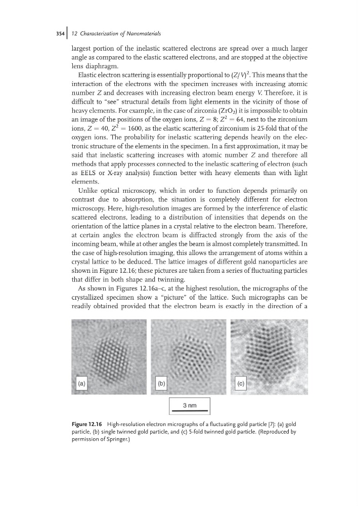
crystal lattice to be deduced. The lattice images of different gold nanoparticles are
shown in Figure 12.16; these pictures are taken from a series of fluctuating particles
that differ in both shape and twinning.
As shown in Figures 12.16a–c, at the highest resolution, the micrographs of the
crystallized specimen show a “picture” of the lattice. Such micrographs can be
readily obtained provided that the electron beam is exactly in the direction of a
Figure 12.16 High-resolution electron micrographs of a fluctuating gold particle [7]: (a) gold
particle, (b) single twinned gold particle, and (c) 5-fold twinned gold particle. (Reproduced by
permission of Springer.)
354j 12 Characterization of Nanomaterials
angle as compared to the elastic scattered electrons, and are stopped at the objective
lens diaphragm.
Elastic electron scattering is essentially proportional to (Z/V)
2
. This means that the
interaction of the electrons with the specimen increases with increasing atomic
number Z and decreases with increasing electron beam energy V. Therefore, it is
difficult to “see” structural details from light elements in the vicinity of those of
heavy elements. For example, in the case of zirconia (ZrO 2 ) it is impossible to obtain
an image of the positions of the oxygen ions, Z ¼ 8; Z
2 ¼ 64, next to the zirconium
ions, Z ¼ 40, Z
2 ¼ 1600, as the elastic scattering of zirconium is 25-fold that of the
oxygen ions. The probability for inelastic scattering depends heavily on the electronic structure of the elements in the specimen. In a first approximation, it may be
said that inelastic scattering increases with atomic number Z and therefore all
methods that apply processes connected to the inelastic scattering of electron (such
as EELS or X-ray analysis) function better with heavy elements than with light
elements.
Unlike optical microscopy, which in order to function depends primarily on
contrast due to absorption, the situation is completely different for electron
microscopy. Here, high-resolution images are formed by the interference of elastic
scattered electrons, leading to a distribution of intensities that depends on the
orientation of the lattice planes in a crystal relative to the electron beam. Therefore,
at certain angles the electron beam is diffracted strongly from the axis of the
incoming beam, while at other angles the beam is almost completely transmitted. In
the case of high-resolution imaging, this allows the arrangement of atoms within a
crystal lattice to be deduced. The lattice images of different gold nanoparticles are
shown in Figure 12.16; these pictures are taken from a series of fluctuating particles
that differ in both shape and twinning.
As shown in Figures 12.16a–c, at the highest resolution, the micrographs of the
crystallized specimen show a “picture” of the lattice. Such micrographs can be
readily obtained provided that the electron beam is exactly in the direction of a
Figure 12.16 High-resolution electron micrographs of a fluctuating gold particle [7]: (a) gold
particle, (b) single twinned gold particle, and (c) 5-fold twinned gold particle. (Reproduced by
permission of Springer.)
354j 12 Characterization of Nanomaterials