

12.4
Electron Microscopy
12.4.1
General Considerations
In order to study the shape, size, and structure of nanoparticles, electron microscopy
is the best-suited technique. Today, however, as electron microscopy is considered a
broad science in its own right, within this chapter we will outline only a few basic
facts, aiming to avoid the impression that simply by reading these few pages it would
be possible to interpret electron micrographs. Electron microscopy is, indeed, a task
for “specialists.”
Roughly speaking, electron microscopy functions like optical microscopy,
except that the difference is simply the application of electron waves instead
of electromagnetic waves. Both types of microscope consist of an illumination
system, a specimen holder, an objective system followed by a projection system,
and finally a registration device. The latter may be either a photographic plate or
an electronic camera system. The need to change from optical microscopy to
electron microscopy lies in the length of the applied waves. According to Abbe, the
minimum feature that can be seen with a conventional optical system is limited by
diffraction to approximately the half of the applied wavelength. In other words, it
is impossible to resolve structural details smaller than half of the wavelength.
Nowadays, optical microscopes come close to the theoretical possible values of the
resolution, but in technical reality in electron microscopes this resolution limit is
by far not achieved.
The resolution of an optical system is limited by the numerical aperture (N A ),
which is, in a good approximation, the ratio of the radius of the lens (which usually is
limited by an aperture diaphragm) over the focal distance. For practical purposes,
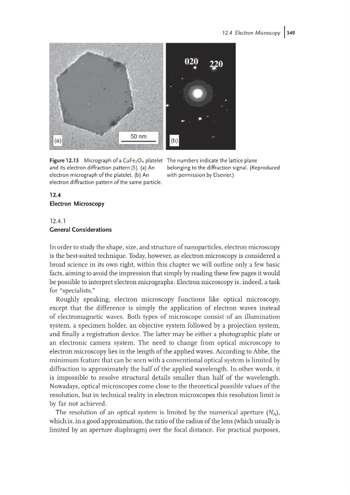
Figure 12.13 Micrograph of a CuFe 2 O 4 platelet
and its electron diffraction pattern [5]. (a) An
electron micrograph of the platelet. (b) An
electron diffraction pattern of the same particle.
The numbers indicate the lattice plane
belonging to the diffraction signal. (Reproduced
with permission by Elsevier.)
12.4 Electron Microscopy j349
Electron Microscopy
12.4.1
General Considerations
In order to study the shape, size, and structure of nanoparticles, electron microscopy
is the best-suited technique. Today, however, as electron microscopy is considered a
broad science in its own right, within this chapter we will outline only a few basic
facts, aiming to avoid the impression that simply by reading these few pages it would
be possible to interpret electron micrographs. Electron microscopy is, indeed, a task
for “specialists.”
Roughly speaking, electron microscopy functions like optical microscopy,
except that the difference is simply the application of electron waves instead
of electromagnetic waves. Both types of microscope consist of an illumination
system, a specimen holder, an objective system followed by a projection system,
and finally a registration device. The latter may be either a photographic plate or
an electronic camera system. The need to change from optical microscopy to
electron microscopy lies in the length of the applied waves. According to Abbe, the
minimum feature that can be seen with a conventional optical system is limited by
diffraction to approximately the half of the applied wavelength. In other words, it
is impossible to resolve structural details smaller than half of the wavelength.
Nowadays, optical microscopes come close to the theoretical possible values of the
resolution, but in technical reality in electron microscopes this resolution limit is
by far not achieved.
The resolution of an optical system is limited by the numerical aperture (N A ),
which is, in a good approximation, the ratio of the radius of the lens (which usually is
limited by an aperture diaphragm) over the focal distance. For practical purposes,
Figure 12.13 Micrograph of a CuFe 2 O 4 platelet
and its electron diffraction pattern [5]. (a) An
electron micrograph of the platelet. (b) An
electron diffraction pattern of the same particle.
The numbers indicate the lattice plane
belonging to the diffraction signal. (Reproduced
with permission by Elsevier.)
12.4 Electron Microscopy j349