

Today, many instruments have the ability to focus the electron beam used for
diffraction to such a large extent that it is possible to obtain the diffraction pattern of
one particle only. An example of this technique, known as selected area diffraction
(SAD), is shown in Figure 12.13. Figure 12.13a shows an electron micrograph of a
CuFe 2 O 4 platelet, a ferrite that crystallizes in the cubic spinel structure, while
Figure 12.13b shows an electron diffraction pattern of exactly this particle. This
precise correlation is important when determining the crystal structure.
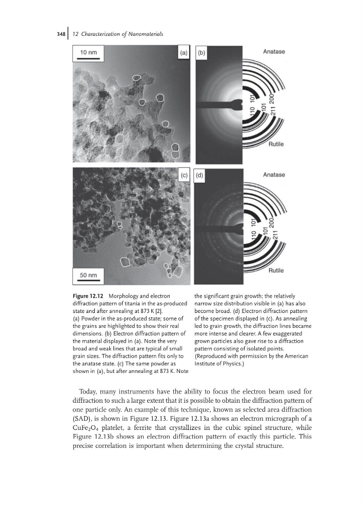
Figure 12.12 Morphology and electron
diffraction pattern of titania in the as-produced
state and after annealing at 873 K [2].
(a) Powder in the as-produced state; some of
the grains are highlighted to show their real
dimensions. (b) Electron diffraction pattern of
the material displayed in (a). Note the very
broad and weak lines that are typical of small
grain sizes. The diffraction pattern fits only to
the anatase state. (c) The same powder as
shown in (a), but after annealing at 873 K. Note
the significant grain growth; the relatively
narrow size distribution visible in (a) has also
become broad. (d) Electron diffraction pattern
of the specimen displayed in (c). As annealing
led to grain growth, the diffraction lines became
more intense and clearer. A few exaggerated
grown particles also gave rise to a diffraction
pattern consisting of isolated points.
(Reproduced with permission by the American
Institute of Physics.)
348j 12 Characterization of Nanomaterials
diffraction to such a large extent that it is possible to obtain the diffraction pattern of
one particle only. An example of this technique, known as selected area diffraction
(SAD), is shown in Figure 12.13. Figure 12.13a shows an electron micrograph of a
CuFe 2 O 4 platelet, a ferrite that crystallizes in the cubic spinel structure, while
Figure 12.13b shows an electron diffraction pattern of exactly this particle. This
precise correlation is important when determining the crystal structure.
Figure 12.12 Morphology and electron
diffraction pattern of titania in the as-produced
state and after annealing at 873 K [2].
(a) Powder in the as-produced state; some of
the grains are highlighted to show their real
dimensions. (b) Electron diffraction pattern of
the material displayed in (a). Note the very
broad and weak lines that are typical of small
grain sizes. The diffraction pattern fits only to
the anatase state. (c) The same powder as
shown in (a), but after annealing at 873 K. Note
the significant grain growth; the relatively
narrow size distribution visible in (a) has also
become broad. (d) Electron diffraction pattern
of the specimen displayed in (c). As annealing
led to grain growth, the diffraction lines became
more intense and clearer. A few exaggerated
grown particles also gave rise to a diffraction
pattern consisting of isolated points.
(Reproduced with permission by the American
Institute of Physics.)
348j 12 Characterization of Nanomaterials