

two orders of magnitude larger. Therefore, for applications in optoelectronics, only
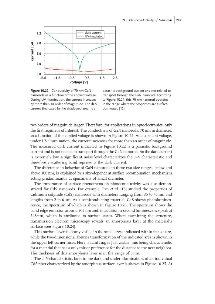
the first regime is of interest. The conductivity of GaN nanorods, 70 nm in diameter,
as a function of the applied voltage is shown in Figure 10.22. At a constant voltage,
under UV illumination, the current increases for more than an order of magnitude.
The measured dark current indicated in Figure 10.22 is a parasitic background
current and is not related to transport through the GaN nanorod. As the dark current
is extremely low, a significant noise level characterizes the I–V characteristic and
therefore a scattering band represents the dark current.
The difference in behavior of GaN nanorods in these two size ranges, below and
above 100 nm, is explained by a size-dependent surface recombination mechanism
acting predominantly at specimens of small diameter.
The importance of surface phenomena on photoconductivity was also demonstrated for CdS nanorods. For example, Pan et al. [13] studied the properties of
cadmium sulphide (CdS) nanorods with diameters ranging from 35 to 45 nm and
lengths from 2 to 6 mm. As a semiconducting material, CdS shows photoluminescence, the spectrum of which is shown in Figure 10.23. The spectrum shows the
band-edge emission around 505 nm and, in addition, a second luminescence peak at
548 nm, which is attributed to surface states. When examining the structure,
transmission electron microscopy reveals an amorphous layer at the material’s
surface (see Figure 10.24).
This surface layer is clearly visible in the small areas indicated within the square,
while the two-dimensional Fourier transformation of the indicated area is shown in
the upper left corner inset. Here, a faint ring is just visible, this being characteristic
for a material that has a only minor preference for the distance to the next neighbor.
The thickness of this amorphous layer is in the range of 3 nm.
The I–V characteristic, both in the dark and under illumination, of an individual
CdS fiber characterized by the amorphous surface layer is shown in Figure 10.25. At
1.2
9.0
6.0
3.0
0.0
1.2
9.0
6.0
3.0
0.0
current [pA]
-2.5
-1.5
-0.5
0.5
1.5
2.5
voltage [V]
dark current
UV-irradiated
Figure 10.22 Conductivity of 70-nm GaN
nanorods as a function of the applied voltage.
During UV illumination, the current increases
by more than an order of magnitude. The dark
current (indicated by the shadowed area) is a
parasitic background current and not related to
transport through the GaN nanorod. According
to Figure 10.21, this 70-nm nanorod operates
in the range where the properties are surfacedominated [12].
10.3 Photoconductivity of Nanorods j285
the first regime is of interest. The conductivity of GaN nanorods, 70 nm in diameter,
as a function of the applied voltage is shown in Figure 10.22. At a constant voltage,
under UV illumination, the current increases for more than an order of magnitude.
The measured dark current indicated in Figure 10.22 is a parasitic background
current and is not related to transport through the GaN nanorod. As the dark current
is extremely low, a significant noise level characterizes the I–V characteristic and
therefore a scattering band represents the dark current.
The difference in behavior of GaN nanorods in these two size ranges, below and
above 100 nm, is explained by a size-dependent surface recombination mechanism
acting predominantly at specimens of small diameter.
The importance of surface phenomena on photoconductivity was also demonstrated for CdS nanorods. For example, Pan et al. [13] studied the properties of
cadmium sulphide (CdS) nanorods with diameters ranging from 35 to 45 nm and
lengths from 2 to 6 mm. As a semiconducting material, CdS shows photoluminescence, the spectrum of which is shown in Figure 10.23. The spectrum shows the
band-edge emission around 505 nm and, in addition, a second luminescence peak at
548 nm, which is attributed to surface states. When examining the structure,
transmission electron microscopy reveals an amorphous layer at the material’s
surface (see Figure 10.24).
This surface layer is clearly visible in the small areas indicated within the square,
while the two-dimensional Fourier transformation of the indicated area is shown in
the upper left corner inset. Here, a faint ring is just visible, this being characteristic
for a material that has a only minor preference for the distance to the next neighbor.
The thickness of this amorphous layer is in the range of 3 nm.
The I–V characteristic, both in the dark and under illumination, of an individual
CdS fiber characterized by the amorphous surface layer is shown in Figure 10.25. At
1.2
9.0
6.0
3.0
0.0
1.2
9.0
6.0
3.0
0.0
current [pA]
-2.5
-1.5
-0.5
0.5
1.5
2.5
voltage [V]
dark current
UV-irradiated
Figure 10.22 Conductivity of 70-nm GaN
nanorods as a function of the applied voltage.
During UV illumination, the current increases
by more than an order of magnitude. The dark
current (indicated by the shadowed area) is a
parasitic background current and not related to
transport through the GaN nanorod. According
to Figure 10.21, this 70-nm nanorod operates
in the range where the properties are surfacedominated [12].
10.3 Photoconductivity of Nanorods j285