

low voltages, this plot is characterized by a linear increase in the current with
increasing voltage, but beyond 5 V a saturation is observed. The difference between
the current in the dark and illuminated states is almost two orders of magnitude.
This remarkable response suggests that CdS would be a good material for the
fabrication of photoelectric and sensing devices.
Calculating the conductance from the values in Figure 10.25 for CdS, whether
illuminated or in the dark, provides interesting insights. In the dark, a decreasing conductance is observed with an increasing applied voltage, whilst at low
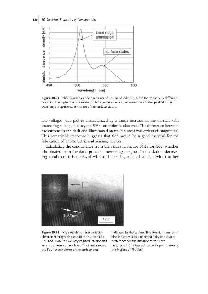
Figure 10.23 Photoluminescence spectrum of CdS nanorods [13]. Note the two clearly different
features. The higher peak is related to band edge emission, whereas the smaller peak at longer
wavelength represents emission of the surface states.
Figure 10.24 High-resolution transmission
electron micrograph close to the surface of a
CdS rod. Note the well-crystallized interior and
an amorphous surface layer. The inset shows
the Fourier transform of the surface area
indicated by the square. This Fourier transform
also indicates a lack of crystallinity and a weak
preference for the distance to the next
neighbors [13]. (Reproduced with permission by
the Institut of Physics.)
286j 10 Electrical Properties of Nanoparticles
increasing voltage, but beyond 5 V a saturation is observed. The difference between
the current in the dark and illuminated states is almost two orders of magnitude.
This remarkable response suggests that CdS would be a good material for the
fabrication of photoelectric and sensing devices.
Calculating the conductance from the values in Figure 10.25 for CdS, whether
illuminated or in the dark, provides interesting insights. In the dark, a decreasing conductance is observed with an increasing applied voltage, whilst at low
Figure 10.23 Photoluminescence spectrum of CdS nanorods [13]. Note the two clearly different
features. The higher peak is related to band edge emission, whereas the smaller peak at longer
wavelength represents emission of the surface states.
Figure 10.24 High-resolution transmission
electron micrograph close to the surface of a
CdS rod. Note the well-crystallized interior and
an amorphous surface layer. The inset shows
the Fourier transform of the surface area
indicated by the square. This Fourier transform
also indicates a lack of crystallinity and a weak
preference for the distance to the next
neighbors [13]. (Reproduced with permission by
the Institut of Physics.)
286j 10 Electrical Properties of Nanoparticles