

to graphene, which is absolutely flat, corrugated. This double bond may also be used
to produce graphene sheets from graphite. One immerses graphite into a solution of
(in the simplest case) formic acid. The small molecules of this compound oxidize the
carbon layers, forming graphene oxide, and attach at these weak points and, at first,
are expanded and, in a second step, defoliate the graphite. The step of oxidation can
also be performed using sulfuric or nitric acid. In the next step, the graphene layers,
now carrying formic acid molecules, are, in the described case, treated with an
alkaline solution for defoliation and afterwards reduced (e.g., using hydrazine). As a
result, one obtains graphene layers suspended in a liquid. Certainly, thermal
reduction is possible, too. A review on graphene synthesis is given by Choi et al. [9].
Carbon nanotubes have many fascinating applications and those employing their
electrical conductivity or high strength are also discussed in Chapters 10 and 11,
respectively. In addition, a small diameter combined with an extreme stiffness
means that carbon nanotubes are ideal materials for the tips used in scanning force
or scanning tunnel microscopes.
Potentially, a major application of nanotubes is as electron emitters. Electron
emission in an electrical field requires a sharp tip; the sharper the tip, the lower the
electrical voltage required for electron emission. This is because the electrical field at
the tip controls electron field emission. Although single-wall nanotubes have the
sharpest tip occurring in nature, in reality multiwall nanotubes are used as they are
more readily available. The emission current of carbon nanotubes as a function of
the applied voltage is shown in Figure 5.22. Two types of nanotube were applied,
namely closed and open. The open nanotubes were obtained by removing the endcaps in an oxidizing medium. The closed nanotubes start emission at 120 V, whereas
the open tubes start significantly later, at 240 V. At 170 V, the emission current is
10
À7 A. Assuming a diameter of about 15 nm, this leads to an electrical current
density in the range of 5:7 Â 10
9 Am
À2 (¼ 5:7 Â 10
3 A mm
À 2 ). Compared to macroscopic metallic electrical conductors, this is an “astronomically ” high current
density and the number would be even higher if the current density were related to
the actual material-containing cross-section of the nanotube. When considering the
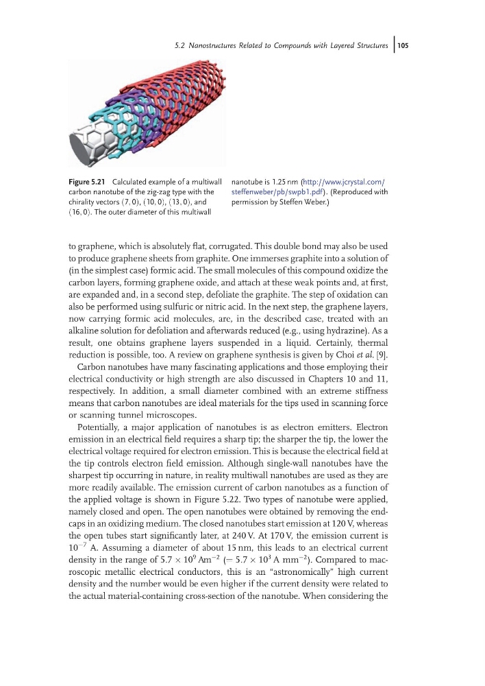
Figure 5.21 Calculated example of a multiwall
carbon nanotube of the zig-zag type with the
chirality vectors 7; 0
ð Þ, 10; 0
ð
Þ, 13; 0
ð
Þ, and
16; 0
ð
Þ. The outer diameter of this multiwall
nanotube is 1.25 nm (http://www.jcrystal.com/
steffenweber/pb/swpb1.pdf ). (Reproduced with
permission by Steffen Weber.)
5.2 Nanostructures Related to Compounds with Layered Structures j105
to produce graphene sheets from graphite. One immerses graphite into a solution of
(in the simplest case) formic acid. The small molecules of this compound oxidize the
carbon layers, forming graphene oxide, and attach at these weak points and, at first,
are expanded and, in a second step, defoliate the graphite. The step of oxidation can
also be performed using sulfuric or nitric acid. In the next step, the graphene layers,
now carrying formic acid molecules, are, in the described case, treated with an
alkaline solution for defoliation and afterwards reduced (e.g., using hydrazine). As a
result, one obtains graphene layers suspended in a liquid. Certainly, thermal
reduction is possible, too. A review on graphene synthesis is given by Choi et al. [9].
Carbon nanotubes have many fascinating applications and those employing their
electrical conductivity or high strength are also discussed in Chapters 10 and 11,
respectively. In addition, a small diameter combined with an extreme stiffness
means that carbon nanotubes are ideal materials for the tips used in scanning force
or scanning tunnel microscopes.
Potentially, a major application of nanotubes is as electron emitters. Electron
emission in an electrical field requires a sharp tip; the sharper the tip, the lower the
electrical voltage required for electron emission. This is because the electrical field at
the tip controls electron field emission. Although single-wall nanotubes have the
sharpest tip occurring in nature, in reality multiwall nanotubes are used as they are
more readily available. The emission current of carbon nanotubes as a function of
the applied voltage is shown in Figure 5.22. Two types of nanotube were applied,
namely closed and open. The open nanotubes were obtained by removing the endcaps in an oxidizing medium. The closed nanotubes start emission at 120 V, whereas
the open tubes start significantly later, at 240 V. At 170 V, the emission current is
10
À7 A. Assuming a diameter of about 15 nm, this leads to an electrical current
density in the range of 5:7 Â 10
9 Am
À2 (¼ 5:7 Â 10
3 A mm
À 2 ). Compared to macroscopic metallic electrical conductors, this is an “astronomically ” high current
density and the number would be even higher if the current density were related to
the actual material-containing cross-section of the nanotube. When considering the
Figure 5.21 Calculated example of a multiwall
carbon nanotube of the zig-zag type with the
chirality vectors 7; 0
ð Þ, 10; 0
ð
Þ, 13; 0
ð
Þ, and
16; 0
ð
Þ. The outer diameter of this multiwall
nanotube is 1.25 nm (http://www.jcrystal.com/
steffenweber/pb/swpb1.pdf ). (Reproduced with
permission by Steffen Weber.)
5.2 Nanostructures Related to Compounds with Layered Structures j105