

9 Mössbauer Spectroscopic Studies on Atomic Diffusion in Materials
505
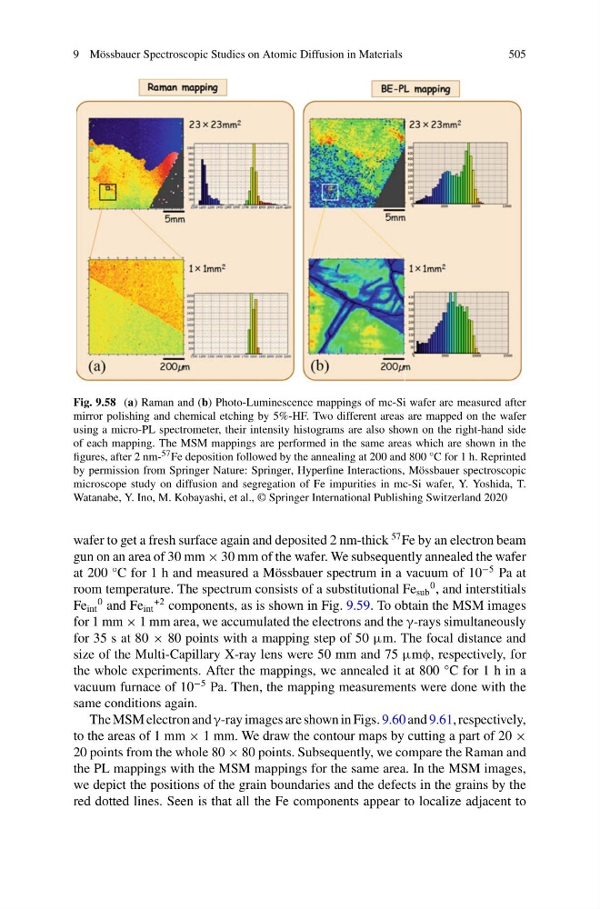
Fig. 9.58 (a) Raman and (b) Photo-Luminescence mappings of mc-Si wafer are measured after
mirror polishing and chemical etching by 5%-HF. Two different areas are mapped on the wafer
using a micro-PL spectrometer, their intensity histograms are also shown on the right-hand side
of each mapping. The MSM mappings are performed in the same areas which are shown in the
figures, after 2 nm- 57 Fe deposition followed by the annealing at 200 and 800 °C for 1 h. Reprinted
by permission from Springer Nature: Springer, Hyperfine Interactions, Mössbauer spectroscopic
microscope study on diffusion and segregation of Fe impurities in mc-Si wafer, Y. Yoshida, T.
Watanabe, Y. Ino, M. Kobayashi, et al., © Springer International Publishing Switzerland 2020
wafer to get a fresh surface again and deposited 2 nm-thick
57 Fe by an electron beam
gun on an area of 30 mm × 30 mm of the wafer. We subsequently annealed the wafer
at 200 °C for 1 h and measured a Mössbauer spectrum in a vacuum of 10
−5 Pa at
room temperature. The spectrum consists of a substitutional Fe sub
0 , and interstitials
Fe int
0 and Fe int
+2 components, as is shown in Fig. 9.59. To obtain the MSM images
for 1 mm × 1 mm area, we accumulated the electrons and the γ-rays simultaneously
for 35 s at 80 × 80 points with a mapping step of 50 μm. The focal distance and
size of the Multi-Capillary X-ray lens were 50 mm and 75 μmφ, respectively, for
the whole experiments. After the mappings, we annealed it at 800 °C for 1 h in a
vacuum furnace of 10
−5 Pa. Then, the mapping measurements were done with the
same conditions again.
The MSM electron and γ-ray images are shown in Figs. 9.60 and 9.61, respectively,
to the areas of 1 mm × 1 mm. We draw the contour maps by cutting a part of 20 ×
20 points from the whole 80 × 80 points. Subsequently, we compare the Raman and
the PL mappings with the MSM mappings for the same area. In the MSM images,
we depict the positions of the grain boundaries and the defects in the grains by the
red dotted lines. Seen is that all the Fe components appear to localize adjacent to
505
Fig. 9.58 (a) Raman and (b) Photo-Luminescence mappings of mc-Si wafer are measured after
mirror polishing and chemical etching by 5%-HF. Two different areas are mapped on the wafer
using a micro-PL spectrometer, their intensity histograms are also shown on the right-hand side
of each mapping. The MSM mappings are performed in the same areas which are shown in the
figures, after 2 nm- 57 Fe deposition followed by the annealing at 200 and 800 °C for 1 h. Reprinted
by permission from Springer Nature: Springer, Hyperfine Interactions, Mössbauer spectroscopic
microscope study on diffusion and segregation of Fe impurities in mc-Si wafer, Y. Yoshida, T.
Watanabe, Y. Ino, M. Kobayashi, et al., © Springer International Publishing Switzerland 2020
wafer to get a fresh surface again and deposited 2 nm-thick
57 Fe by an electron beam
gun on an area of 30 mm × 30 mm of the wafer. We subsequently annealed the wafer
at 200 °C for 1 h and measured a Mössbauer spectrum in a vacuum of 10
−5 Pa at
room temperature. The spectrum consists of a substitutional Fe sub
0 , and interstitials
Fe int
0 and Fe int
+2 components, as is shown in Fig. 9.59. To obtain the MSM images
for 1 mm × 1 mm area, we accumulated the electrons and the γ-rays simultaneously
for 35 s at 80 × 80 points with a mapping step of 50 μm. The focal distance and
size of the Multi-Capillary X-ray lens were 50 mm and 75 μmφ, respectively, for
the whole experiments. After the mappings, we annealed it at 800 °C for 1 h in a
vacuum furnace of 10
−5 Pa. Then, the mapping measurements were done with the
same conditions again.
The MSM electron and γ-ray images are shown in Figs. 9.60 and 9.61, respectively,
to the areas of 1 mm × 1 mm. We draw the contour maps by cutting a part of 20 ×
20 points from the whole 80 × 80 points. Subsequently, we compare the Raman and
the PL mappings with the MSM mappings for the same area. In the MSM images,
we depict the positions of the grain boundaries and the defects in the grains by the
red dotted lines. Seen is that all the Fe components appear to localize adjacent to