

504
Y. Yoshida
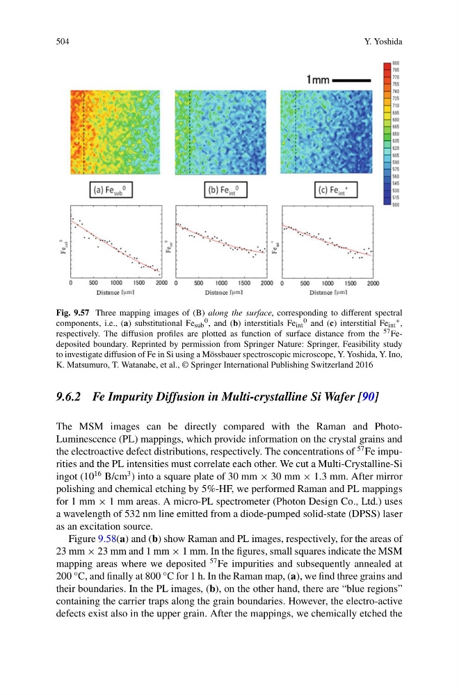
Fig. 9.57 Three mapping images of (B) along the surface, corresponding to different spectral
components, i.e., (a) substitutional Fe sub
0 , and (b) interstitials Fe int
0 and (c) interstitial Fe int
+ ,
respectively. The diffusion profiles are plotted as function of surface distance from the 57 Fedeposited boundary. Reprinted by permission from Springer Nature: Springer, Feasibility study
to investigate diffusion of Fe in Si using a Mössbauer spectroscopic microscope, Y. Yoshida, Y. Ino,
K. Matsumuro, T. Watanabe, et al., © Springer International Publishing Switzerland 2016
9.6.2 Fe Impurity Diffusion in Multi-crystalline Si Wafer [90]
The MSM images can be directly compared with the Raman and PhotoLuminescence (PL) mappings, which provide information on the crystal grains and
the electroactive defect distributions, respectively. The concentrations of
57 Fe impurities and the PL intensities must correlate each other. We cut a Multi-Crystalline-Si
ingot (10
16 B/cm
3 ) into a square plate of 30 mm × 30 mm × 1.3 mm. After mirror
polishing and chemical etching by 5%-HF, we performed Raman and PL mappings
for 1 mm × 1 mm areas. A micro-PL spectrometer (Photon Design Co., Ltd.) uses
a wavelength of 532 nm line emitted from a diode-pumped solid-state (DPSS) laser
as an excitation source.
Figure 9.58(a) and (b) show Raman and PL images, respectively, for the areas of
23 mm × 23 mm and 1 mm × 1 mm. In the figures, small squares indicate the MSM
mapping areas where we deposited
57 Fe impurities and subsequently annealed at
200 °C, and finally at 800 °C for 1 h. In the Raman map, (a), we find three grains and
their boundaries. In the PL images, (b), on the other hand, there are “blue regions”
containing the carrier traps along the grain boundaries. However, the electro-active
defects exist also in the upper grain. After the mappings, we chemically etched the
Y. Yoshida
Fig. 9.57 Three mapping images of (B) along the surface, corresponding to different spectral
components, i.e., (a) substitutional Fe sub
0 , and (b) interstitials Fe int
0 and (c) interstitial Fe int
+ ,
respectively. The diffusion profiles are plotted as function of surface distance from the 57 Fedeposited boundary. Reprinted by permission from Springer Nature: Springer, Feasibility study
to investigate diffusion of Fe in Si using a Mössbauer spectroscopic microscope, Y. Yoshida, Y. Ino,
K. Matsumuro, T. Watanabe, et al., © Springer International Publishing Switzerland 2016
9.6.2 Fe Impurity Diffusion in Multi-crystalline Si Wafer [90]
The MSM images can be directly compared with the Raman and PhotoLuminescence (PL) mappings, which provide information on the crystal grains and
the electroactive defect distributions, respectively. The concentrations of
57 Fe impurities and the PL intensities must correlate each other. We cut a Multi-Crystalline-Si
ingot (10
16 B/cm
3 ) into a square plate of 30 mm × 30 mm × 1.3 mm. After mirror
polishing and chemical etching by 5%-HF, we performed Raman and PL mappings
for 1 mm × 1 mm areas. A micro-PL spectrometer (Photon Design Co., Ltd.) uses
a wavelength of 532 nm line emitted from a diode-pumped solid-state (DPSS) laser
as an excitation source.
Figure 9.58(a) and (b) show Raman and PL images, respectively, for the areas of
23 mm × 23 mm and 1 mm × 1 mm. In the figures, small squares indicate the MSM
mapping areas where we deposited
57 Fe impurities and subsequently annealed at
200 °C, and finally at 800 °C for 1 h. In the Raman map, (a), we find three grains and
their boundaries. In the PL images, (b), on the other hand, there are “blue regions”
containing the carrier traps along the grain boundaries. However, the electro-active
defects exist also in the upper grain. After the mappings, we chemically etched the