

496
Y. Yoshida
inversed pole figure map along a normal direction of EBSD. The crystal orientation
refers to as the colour distribution in the unit triangle pole figure inserted at a lower
right-hand side of the Figure. In this region, there are the twin boundaries of 3, the
coincidence boundaries of high such as 35a, and the random boundaries (R).
Figure 9.49(e) shows a local misorientation map relating to the residual strains. This
image indicates large strains at a particular region in the grain and at a location near
the electrode.
Our set-up provides a possibility to get a 3D-mapping image by combining the
2D-mapping with the depth profiles, which can be measured by an Electron Spectrometer (HV-CSA, FOCUS). The conversion and Auger electrons are emitted from
the
57 Fe nucleus distributing at a different depth from the surface. Subsequently, the
electrons lose their energy due to the inelastic collisions, which can be measured
by the spectrometer. Therefore, it is possible to obtain a depth distribution of
57 Fe
atoms by selecting the energies of the electrons, yielding a possibility for a depth
selective mapping. This technique is called a depth selective conversion Mössbauer
spectroscopy (DSCEMS) with the probing depth of about 100 nm, and the depth
resolution of 5–10 nm for
57 Fe. Previously, we measured for the sample with the
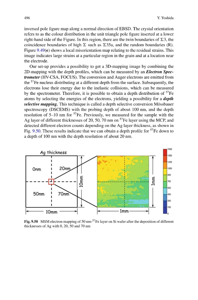
Ag layer of different thicknesses of 20, 50, 70 nm on
57 Fe layer using the MCP, and
detected different electron counts depending on the Ag layer thickness, as shown in
Fig. 9.50. These results indicate that we can obtain a depth profile for
57 Fe down to
a depth of 100 nm with the depth resolution of about 20 nm.
Fig. 9.50 MSM electron mapping of 50 nm- 57 Fe layer on Si wafer after the deposition of different
thicknesses of Ag with 0, 20, 50 and 70 nm
Y. Yoshida
inversed pole figure map along a normal direction of EBSD. The crystal orientation
refers to as the colour distribution in the unit triangle pole figure inserted at a lower
right-hand side of the Figure. In this region, there are the twin boundaries of 3, the
coincidence boundaries of high such as 35a, and the random boundaries (R).
Figure 9.49(e) shows a local misorientation map relating to the residual strains. This
image indicates large strains at a particular region in the grain and at a location near
the electrode.
Our set-up provides a possibility to get a 3D-mapping image by combining the
2D-mapping with the depth profiles, which can be measured by an Electron Spectrometer (HV-CSA, FOCUS). The conversion and Auger electrons are emitted from
the
57 Fe nucleus distributing at a different depth from the surface. Subsequently, the
electrons lose their energy due to the inelastic collisions, which can be measured
by the spectrometer. Therefore, it is possible to obtain a depth distribution of
57 Fe
atoms by selecting the energies of the electrons, yielding a possibility for a depth
selective mapping. This technique is called a depth selective conversion Mössbauer
spectroscopy (DSCEMS) with the probing depth of about 100 nm, and the depth
resolution of 5–10 nm for
57 Fe. Previously, we measured for the sample with the
Ag layer of different thicknesses of 20, 50, 70 nm on
57 Fe layer using the MCP, and
detected different electron counts depending on the Ag layer thickness, as shown in
Fig. 9.50. These results indicate that we can obtain a depth profile for
57 Fe down to
a depth of 100 nm with the depth resolution of about 20 nm.
Fig. 9.50 MSM electron mapping of 50 nm- 57 Fe layer on Si wafer after the deposition of different
thicknesses of Ag with 0, 20, 50 and 70 nm