

7.3 Using the IEEE Std. 1500 Standard in Order …
671
7.3.4 IIPS Module Structure
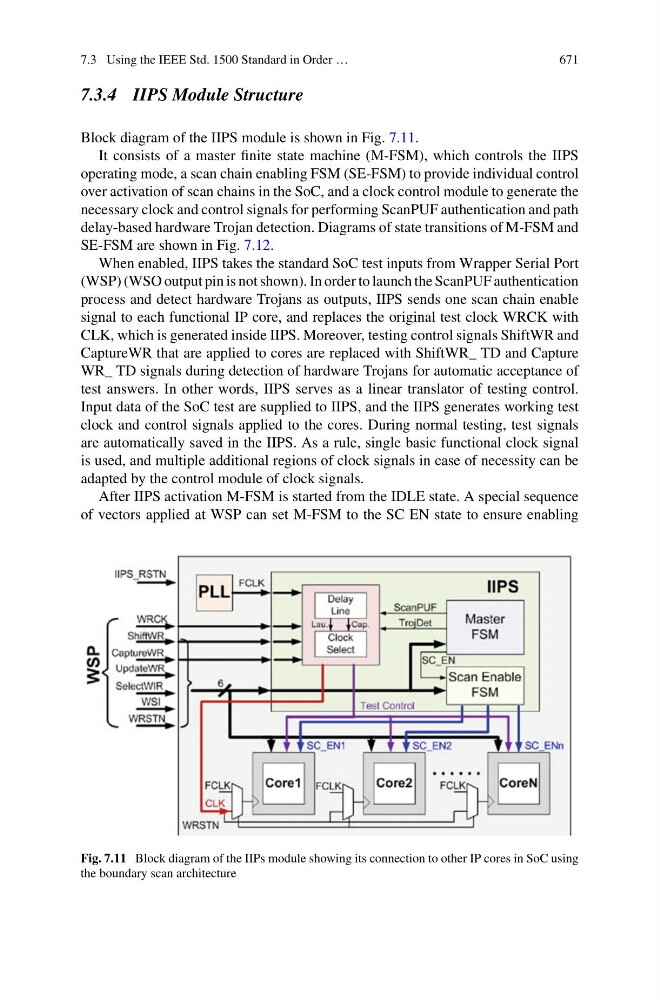
Block diagram of the IIPS module is shown in Fig. 7.11.
It consists of a master finite state machine (M-FSM), which controls the IIPS
operating mode, a scan chain enabling FSM (SE-FSM) to provide individual control
over activation of scan chains in the SoC, and a clock control module to generate the
necessary clock and control signals for performing ScanPUF authentication and path
delay-based hardware Trojan detection. Diagrams of state transitions of M-FSM and
SE-FSM are shown in Fig. 7.12.
When enabled, IIPS takes the standard SoC test inputs from Wrapper Serial Port
(WSP) (WSO output pin is not shown). In order to launch the ScanPUF authentication
process and detect hardware Trojans as outputs, IIPS sends one scan chain enable
signal to each functional IP core, and replaces the original test clock WRCK with
CLK, which is generated inside IIPS. Moreover, testing control signals ShiftWR and
CaptureWR that are applied to cores are replaced with ShiftWR_ TD and Capture
WR_ TD signals during detection of hardware Trojans for automatic acceptance of
test answers. In other words, IIPS serves as a linear translator of testing control.
Input data of the SoC test are supplied to IIPS, and the IIPS generates working test
clock and control signals applied to the cores. During normal testing, test signals
are automatically saved in the IIPS. As a rule, single basic functional clock signal
is used, and multiple additional regions of clock signals in case of necessity can be
adapted by the control module of clock signals.
After IIPS activation M-FSM is started from the IDLE state. A special sequence
of vectors applied at WSP can set M-FSM to the SC EN state to ensure enabling
Fig. 7.11 Block diagram of the IIPs module showing its connection to other IP cores in SoC using
the boundary scan architecture