

618
6 Reverse Engineering of Microcircuits
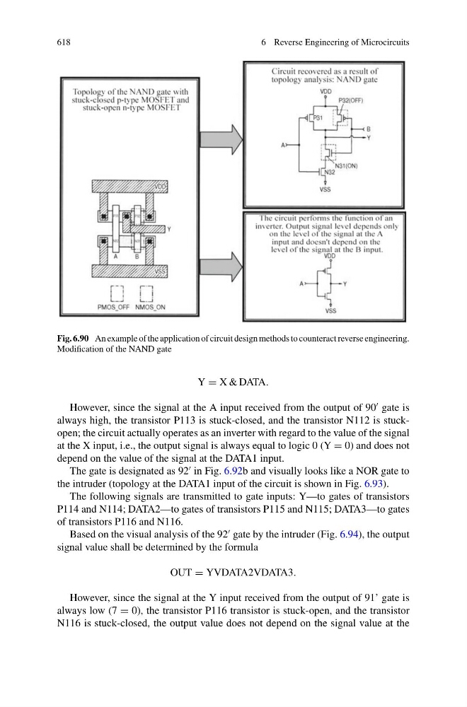
Fig. 6.90 An example of the application of circuit design methods to counteract reverse engineering.
Modification of the NAND gate
Y = X & DATA.
However, since the signal at the A input received from the output of 90
gate is
always high, the transistor P113 is stuck-closed, and the transistor N112 is stuckopen; the circuit actually operates as an inverter with regard to the value of the signal
at the X input, i.e., the output signal is always equal to logic 0 (Y = 0) and does not
depend on the value of the signal at the DATA1 input.
The gate is designated as 92
in Fig. 6.92b and visually looks like a NOR gate to
the intruder (topology at the DATA1 input of the circuit is shown in Fig. 6.93).
The following signals are transmitted to gate inputs: Y—to gates of transistors
P114 and N114; DATA2—to gates of transistors P115 and N115; DATA3—to gates
of transistors P116 and N116.
Based on the visual analysis of the 92
gate by the intruder (Fig. 6.94), the output
signal value shall be determined by the formula
OUT = YVDATA2VDATA3.
However, since the signal at the Y input received from the output of 91’ gate is
always low (7 = 0), the transistor P116 transistor is stuck-open, and the transistor
N116 is stuck-closed, the output value does not depend on the signal value at the
6 Reverse Engineering of Microcircuits
Fig. 6.90 An example of the application of circuit design methods to counteract reverse engineering.
Modification of the NAND gate
Y = X & DATA.
However, since the signal at the A input received from the output of 90
gate is
always high, the transistor P113 is stuck-closed, and the transistor N112 is stuckopen; the circuit actually operates as an inverter with regard to the value of the signal
at the X input, i.e., the output signal is always equal to logic 0 (Y = 0) and does not
depend on the value of the signal at the DATA1 input.
The gate is designated as 92
in Fig. 6.92b and visually looks like a NOR gate to
the intruder (topology at the DATA1 input of the circuit is shown in Fig. 6.93).
The following signals are transmitted to gate inputs: Y—to gates of transistors
P114 and N114; DATA2—to gates of transistors P115 and N115; DATA3—to gates
of transistors P116 and N116.
Based on the visual analysis of the 92
gate by the intruder (Fig. 6.94), the output
signal value shall be determined by the formula
OUT = YVDATA2VDATA3.
However, since the signal at the Y input received from the output of 91’ gate is
always low (7 = 0), the transistor P116 transistor is stuck-open, and the transistor
N116 is stuck-closed, the output value does not depend on the signal value at the