

6.7 Methods of Counteracting Microcircuit Re-engineering Processes
619
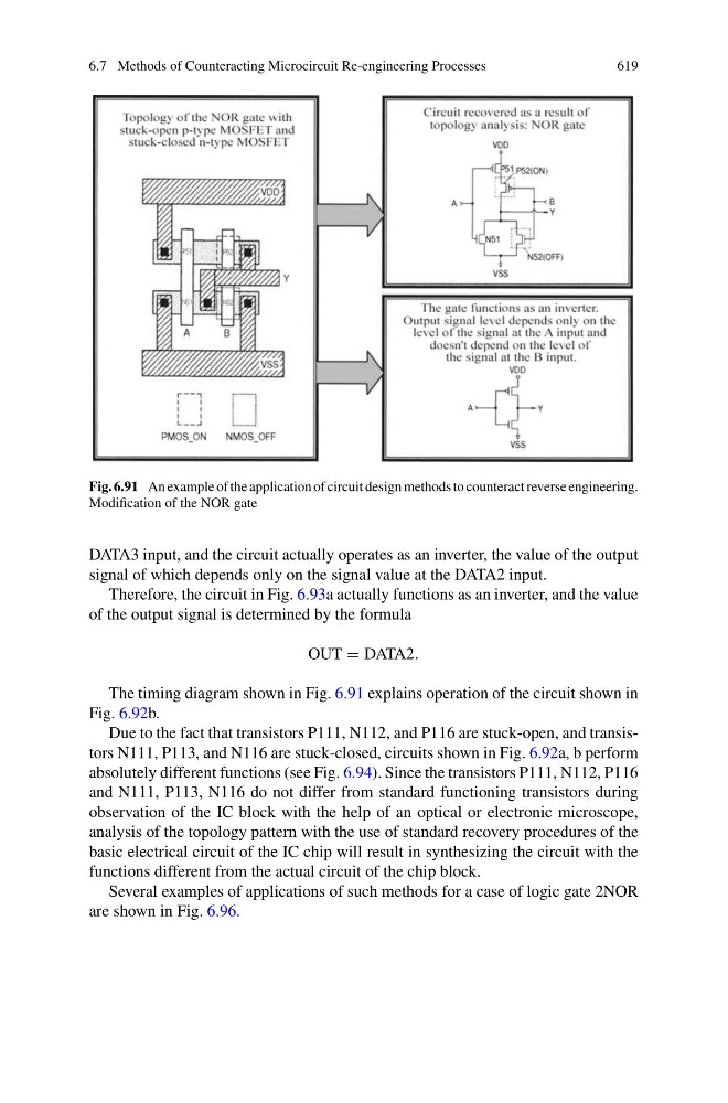
Fig. 6.91 An example of the application of circuit design methods to counteract reverse engineering.
Modification of the NOR gate
DATA3 input, and the circuit actually operates as an inverter, the value of the output
signal of which depends only on the signal value at the DATA2 input.
Therefore, the circuit in Fig. 6.93a actually functions as an inverter, and the value
of the output signal is determined by the formula
OUT = DATA2.
The timing diagram shown in Fig. 6.91 explains operation of the circuit shown in
Fig. 6.92b.
Due to the fact that transistors P111, N112, and P116 are stuck-open, and transistors N111, P113, and N116 are stuck-closed, circuits shown in Fig. 6.92a, b perform
absolutely different functions (see Fig. 6.94). Since the transistors P111, N112, P116
and N111, P113, N116 do not differ from standard functioning transistors during
observation of the IC block with the help of an optical or electronic microscope,
analysis of the topology pattern with the use of standard recovery procedures of the
basic electrical circuit of the IC chip will result in synthesizing the circuit with the
functions different from the actual circuit of the chip block.
Several examples of applications of such methods for a case of logic gate 2NOR
are shown in Fig. 6.96.
619
Fig. 6.91 An example of the application of circuit design methods to counteract reverse engineering.
Modification of the NOR gate
DATA3 input, and the circuit actually operates as an inverter, the value of the output
signal of which depends only on the signal value at the DATA2 input.
Therefore, the circuit in Fig. 6.93a actually functions as an inverter, and the value
of the output signal is determined by the formula
OUT = DATA2.
The timing diagram shown in Fig. 6.91 explains operation of the circuit shown in
Fig. 6.92b.
Due to the fact that transistors P111, N112, and P116 are stuck-open, and transistors N111, P113, and N116 are stuck-closed, circuits shown in Fig. 6.92a, b perform
absolutely different functions (see Fig. 6.94). Since the transistors P111, N112, P116
and N111, P113, N116 do not differ from standard functioning transistors during
observation of the IC block with the help of an optical or electronic microscope,
analysis of the topology pattern with the use of standard recovery procedures of the
basic electrical circuit of the IC chip will result in synthesizing the circuit with the
functions different from the actual circuit of the chip block.
Several examples of applications of such methods for a case of logic gate 2NOR
are shown in Fig. 6.96.