

6.7 Methods of Counteracting Microcircuit Re-engineering Processes
617
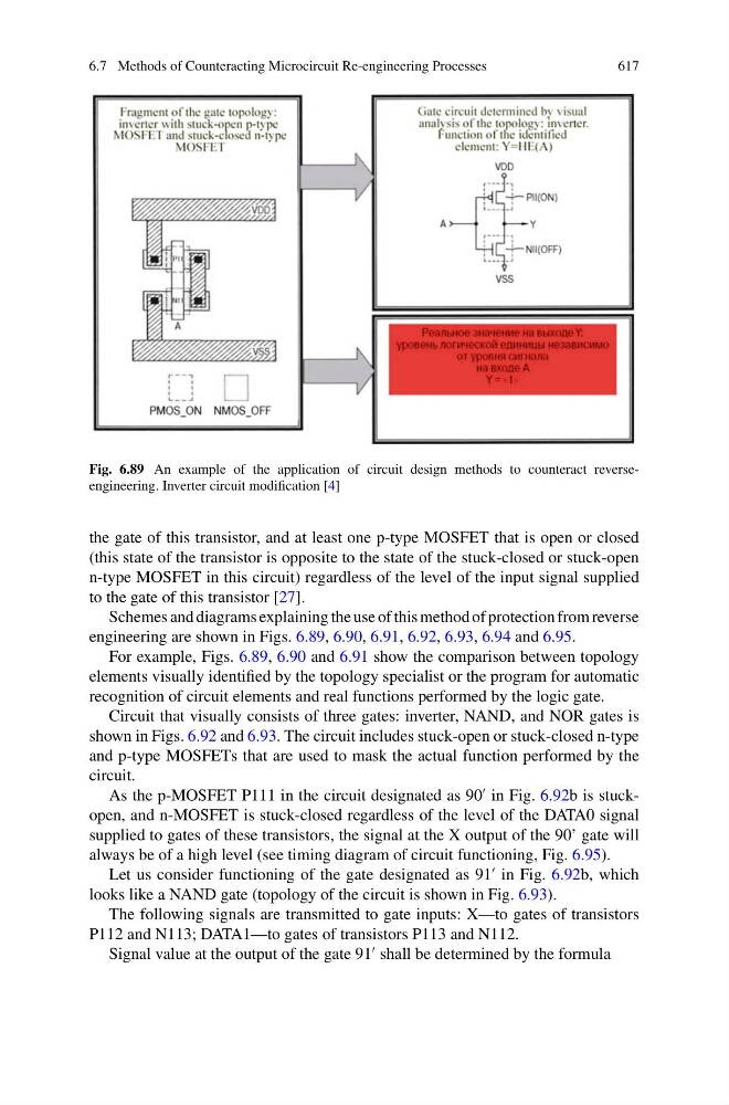
Fig. 6.89 An example of the application of circuit design methods to counteract reverseengineering. Inverter circuit modification [4]
the gate of this transistor, and at least one p-type MOSFET that is open or closed
(this state of the transistor is opposite to the state of the stuck-closed or stuck-open
n-type MOSFET in this circuit) regardless of the level of the input signal supplied
to the gate of this transistor [27].
Schemes and diagrams explaining the use of this method of protection from reverse
engineering are shown in Figs. 6.89, 6.90, 6.91, 6.92, 6.93, 6.94 and 6.95.
For example, Figs. 6.89, 6.90 and 6.91 show the comparison between topology
elements visually identified by the topology specialist or the program for automatic
recognition of circuit elements and real functions performed by the logic gate.
Circuit that visually consists of three gates: inverter, NAND, and NOR gates is
shown in Figs. 6.92 and 6.93. The circuit includes stuck-open or stuck-closed n-type
and p-type MOSFETs that are used to mask the actual function performed by the
circuit.
As the p-MOSFET P111 in the circuit designated as 90
in Fig. 6.92b is stuckopen, and n-MOSFET is stuck-closed regardless of the level of the DATA0 signal
supplied to gates of these transistors, the signal at the X output of the 90’ gate will
always be of a high level (see timing diagram of circuit functioning, Fig. 6.95).
Let us consider functioning of the gate designated as 91
in Fig. 6.92b, which
looks like a NAND gate (topology of the circuit is shown in Fig. 6.93).
The following signals are transmitted to gate inputs: X—to gates of transistors
P112 and N113; DATA1—to gates of transistors P113 and N112.
Signal value at the output of the gate 91
shall be determined by the formula
617
Fig. 6.89 An example of the application of circuit design methods to counteract reverseengineering. Inverter circuit modification [4]
the gate of this transistor, and at least one p-type MOSFET that is open or closed
(this state of the transistor is opposite to the state of the stuck-closed or stuck-open
n-type MOSFET in this circuit) regardless of the level of the input signal supplied
to the gate of this transistor [27].
Schemes and diagrams explaining the use of this method of protection from reverse
engineering are shown in Figs. 6.89, 6.90, 6.91, 6.92, 6.93, 6.94 and 6.95.
For example, Figs. 6.89, 6.90 and 6.91 show the comparison between topology
elements visually identified by the topology specialist or the program for automatic
recognition of circuit elements and real functions performed by the logic gate.
Circuit that visually consists of three gates: inverter, NAND, and NOR gates is
shown in Figs. 6.92 and 6.93. The circuit includes stuck-open or stuck-closed n-type
and p-type MOSFETs that are used to mask the actual function performed by the
circuit.
As the p-MOSFET P111 in the circuit designated as 90
in Fig. 6.92b is stuckopen, and n-MOSFET is stuck-closed regardless of the level of the DATA0 signal
supplied to gates of these transistors, the signal at the X output of the 90’ gate will
always be of a high level (see timing diagram of circuit functioning, Fig. 6.95).
Let us consider functioning of the gate designated as 91
in Fig. 6.92b, which
looks like a NAND gate (topology of the circuit is shown in Fig. 6.93).
The following signals are transmitted to gate inputs: X—to gates of transistors
P112 and N113; DATA1—to gates of transistors P113 and N112.
Signal value at the output of the gate 91
shall be determined by the formula