

614
6 Reverse Engineering of Microcircuits
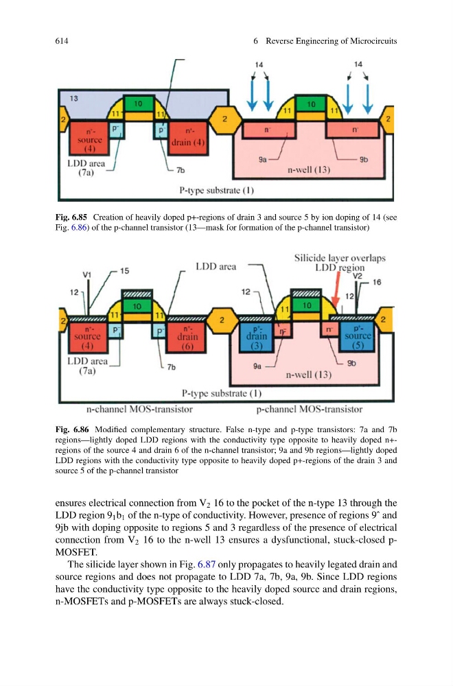
Fig. 6.85 Creation of heavily doped p+-regions of drain 3 and source 5 by ion doping of 14 (see
Fig. 6.86) of the p-channel transistor (13—mask for formation of the p-channel transistor)
Fig. 6.86 Modified complementary structure. False n-type and p-type transistors: 7a and 7b
regions—lightly doped LDD regions with the conductivity type opposite to heavily doped n+regions of the source 4 and drain 6 of the n-channel transistor; 9a and 9b regions—lightly doped
LDD regions with the conductivity type opposite to heavily doped p+-regions of the drain 3 and
source 5 of the p-channel transistor
ensures electrical connection from V 2 16 to the pocket of the n-type 13 through the
LDD region 9 1 b 1 of the n-type of conductivity. However, presence of regions 9ˆ and
9jb with doping opposite to regions 5 and 3 regardless of the presence of electrical
connection from V 2 16 to the n-well 13 ensures a dysfunctional, stuck-closed pMOSFET.
The silicide layer shown in Fig. 6.87 only propagates to heavily legated drain and
source regions and does not propagate to LDD 7a, 7b, 9a, 9b. Since LDD regions
have the conductivity type opposite to the heavily doped source and drain regions,
n-MOSFETs and p-MOSFETs are always stuck-closed.
6 Reverse Engineering of Microcircuits
Fig. 6.85 Creation of heavily doped p+-regions of drain 3 and source 5 by ion doping of 14 (see
Fig. 6.86) of the p-channel transistor (13—mask for formation of the p-channel transistor)
Fig. 6.86 Modified complementary structure. False n-type and p-type transistors: 7a and 7b
regions—lightly doped LDD regions with the conductivity type opposite to heavily doped n+regions of the source 4 and drain 6 of the n-channel transistor; 9a and 9b regions—lightly doped
LDD regions with the conductivity type opposite to heavily doped p+-regions of the drain 3 and
source 5 of the p-channel transistor
ensures electrical connection from V 2 16 to the pocket of the n-type 13 through the
LDD region 9 1 b 1 of the n-type of conductivity. However, presence of regions 9ˆ and
9jb with doping opposite to regions 5 and 3 regardless of the presence of electrical
connection from V 2 16 to the n-well 13 ensures a dysfunctional, stuck-closed pMOSFET.
The silicide layer shown in Fig. 6.87 only propagates to heavily legated drain and
source regions and does not propagate to LDD 7a, 7b, 9a, 9b. Since LDD regions
have the conductivity type opposite to the heavily doped source and drain regions,
n-MOSFETs and p-MOSFETs are always stuck-closed.