

6.7 Methods of Counteracting Microcircuit Re-engineering Processes
613
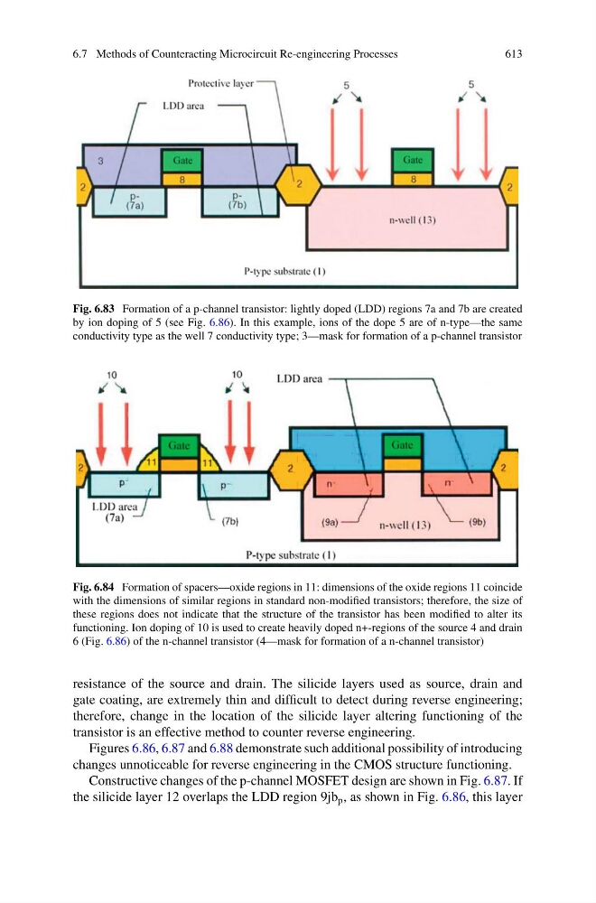
Fig. 6.83 Formation of a p-channel transistor: lightly doped (LDD) regions 7a and 7b are created
by ion doping of 5 (see Fig. 6.86). In this example, ions of the dope 5 are of n-type—the same
conductivity type as the well 7 conductivity type; 3—mask for formation of a p-channel transistor
Fig. 6.84 Formation of spacers—oxide regions in 11: dimensions of the oxide regions 11 coincide
with the dimensions of similar regions in standard non-modified transistors; therefore, the size of
these regions does not indicate that the structure of the transistor has been modified to alter its
functioning. Ion doping of 10 is used to create heavily doped n+-regions of the source 4 and drain
6 (Fig. 6.86) of the n-channel transistor (4—mask for formation of a n-channel transistor)
resistance of the source and drain. The silicide layers used as source, drain and
gate coating, are extremely thin and difficult to detect during reverse engineering;
therefore, change in the location of the silicide layer altering functioning of the
transistor is an effective method to counter reverse engineering.
Figures 6.86, 6.87 and 6.88 demonstrate such additional possibility of introducing
changes unnoticeable for reverse engineering in the CMOS structure functioning.
Constructive changes of the p-channel MOSFET design are shown in Fig. 6.87. If
the silicide layer 12 overlaps the LDD region 9jb p , as shown in Fig. 6.86, this layer
613
Fig. 6.83 Formation of a p-channel transistor: lightly doped (LDD) regions 7a and 7b are created
by ion doping of 5 (see Fig. 6.86). In this example, ions of the dope 5 are of n-type—the same
conductivity type as the well 7 conductivity type; 3—mask for formation of a p-channel transistor
Fig. 6.84 Formation of spacers—oxide regions in 11: dimensions of the oxide regions 11 coincide
with the dimensions of similar regions in standard non-modified transistors; therefore, the size of
these regions does not indicate that the structure of the transistor has been modified to alter its
functioning. Ion doping of 10 is used to create heavily doped n+-regions of the source 4 and drain
6 (Fig. 6.86) of the n-channel transistor (4—mask for formation of a n-channel transistor)
resistance of the source and drain. The silicide layers used as source, drain and
gate coating, are extremely thin and difficult to detect during reverse engineering;
therefore, change in the location of the silicide layer altering functioning of the
transistor is an effective method to counter reverse engineering.
Figures 6.86, 6.87 and 6.88 demonstrate such additional possibility of introducing
changes unnoticeable for reverse engineering in the CMOS structure functioning.
Constructive changes of the p-channel MOSFET design are shown in Fig. 6.87. If
the silicide layer 12 overlaps the LDD region 9jb p , as shown in Fig. 6.86, this layer