

612
6 Reverse Engineering of Microcircuits
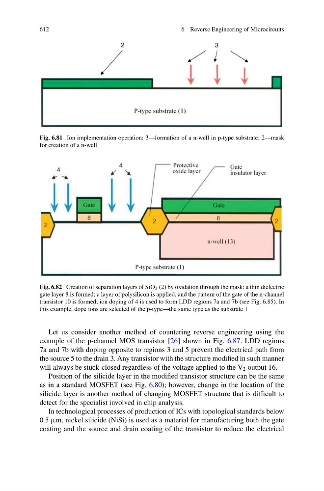
Fig. 6.81 Ion implementation operation: 3—formation of a n-well in p-type substrate; 2—mask
for creation of a n-well
Fig. 6.82 Creation of separation layers of SiO 2 (2) by oxidation through the mask: a thin dielectric
gate layer 8 is formed; a layer of polysilicon is applied, and the pattern of the gate of the n-channel
transistor 10 is formed; ion doping of 4 is used to form LDD regions 7a and 7b (see Fig. 6.85). In
this example, dope ions are selected of the p-type—the same type as the substrate 1
Let us consider another method of countering reverse engineering using the
example of the p-channel MOS transistor [26] shown in Fig. 6.87. LDD regions
7a and 7b with doping opposite to regions 3 and 5 prevent the electrical path from
the source 5 to the drain 3. Any transistor with the structure modified in such manner
will always be stuck-closed regardless of the voltage applied to the V 2 output 16.
Position of the silicide layer in the modified transistor structure can be the same
as in a standard MOSFET (see Fig. 6.80); however, change in the location of the
silicide layer is another method of changing MOSFET structure that is difficult to
detect for the specialist involved in chip analysis.
In technological processes of production of ICs with topological standards below
0.5 μm, nickel silicide (NiSi) is used as a material for manufacturing both the gate
coating and the source and drain coating of the transistor to reduce the electrical
6 Reverse Engineering of Microcircuits
Fig. 6.81 Ion implementation operation: 3—formation of a n-well in p-type substrate; 2—mask
for creation of a n-well
Fig. 6.82 Creation of separation layers of SiO 2 (2) by oxidation through the mask: a thin dielectric
gate layer 8 is formed; a layer of polysilicon is applied, and the pattern of the gate of the n-channel
transistor 10 is formed; ion doping of 4 is used to form LDD regions 7a and 7b (see Fig. 6.85). In
this example, dope ions are selected of the p-type—the same type as the substrate 1
Let us consider another method of countering reverse engineering using the
example of the p-channel MOS transistor [26] shown in Fig. 6.87. LDD regions
7a and 7b with doping opposite to regions 3 and 5 prevent the electrical path from
the source 5 to the drain 3. Any transistor with the structure modified in such manner
will always be stuck-closed regardless of the voltage applied to the V 2 output 16.
Position of the silicide layer in the modified transistor structure can be the same
as in a standard MOSFET (see Fig. 6.80); however, change in the location of the
silicide layer is another method of changing MOSFET structure that is difficult to
detect for the specialist involved in chip analysis.
In technological processes of production of ICs with topological standards below
0.5 μm, nickel silicide (NiSi) is used as a material for manufacturing both the gate
coating and the source and drain coating of the transistor to reduce the electrical